
Electrical and Network Management in High-Level Autonomous Driving System Architecture
Author | Orchid
During the architectural design of high-level autonomous driving systems, the internal architecture of their domain control generally involves main controller chip MCU, computing chip SOC, power management module chip PMIC, codecs, CAN transceivers, network switches, and so on. These design elements are not simply hardware connections at the bottom level, but rather they also require corresponding software and hardware module development for network configuration, power management, storage configuration, and so on from a software perspective. Among them, power configuration and network boot configuration have always been parts of the high-level domain control design content that system architects, hardware architects, and software architects need to overcome.
This article will provide detailed explanations of power management and network management using a typical system architecture constructed with a popular power management chip, PMIC, in the industry. This includes the power distribution network (PDN) between two PMIC power management modules (a typical TPS6594-Q1 device), as well as the DRA829V (TI’s DRA829V is a dual Arm® Cortex®-A72, quad-core Cortex®-R5F, an 8-port Ethernet and 4-port PCIe switch) or TDA4VM (a smart driving domain control SOC processor) equipped with an independent MCU and main power rails.
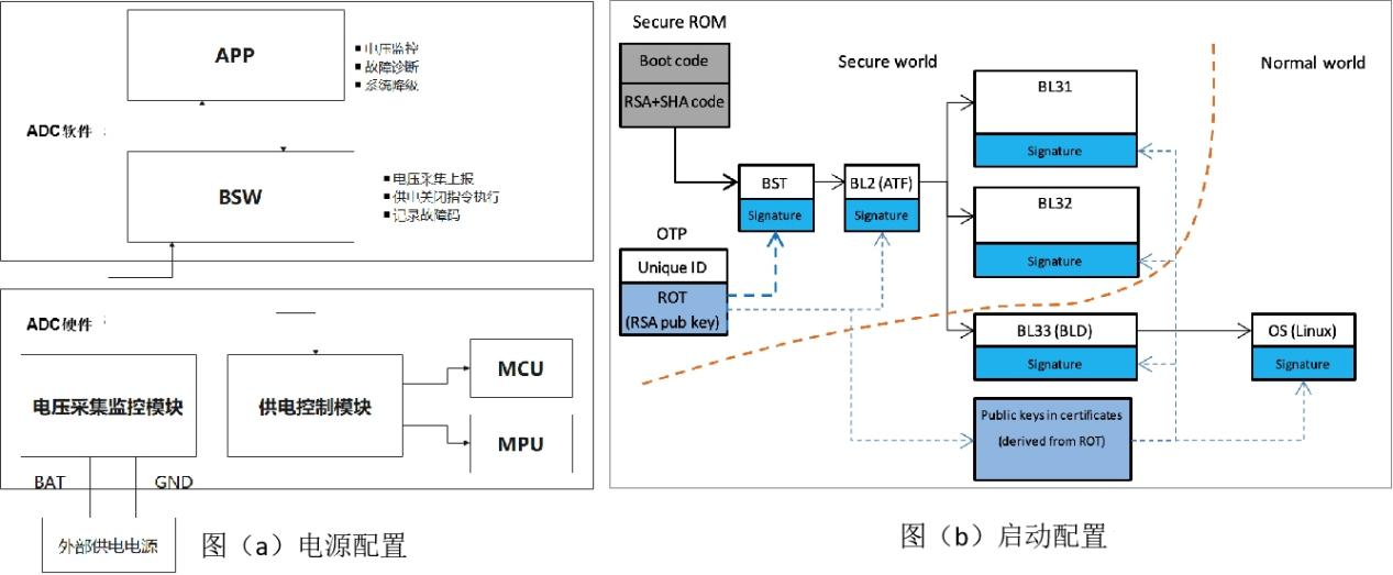
The TDA4 series chip can be considered a classic lower-level version of a heterogeneous chip, and its corresponding internal processor can act as an independent security monitor (MCU safety island) resource for the main processor, ensuring the secure operation of the system. The MCU processor must maintain minimal system manipulation ability (also known as MCU Only mode) to significantly reduce processor power consumption, thereby extending battery life during standby use cases and reducing component temperature.
Power Management Profiles in Different Smart Driving System ArchitecturesOf course, the usage and scenarios of ADAS system chips vary depending on their application needs. As a primary version of heterogenous chips, L2 level usually requires a computing power of 5 TOPS, L3 level requires 100+ TOPS and L4 level requires 300+ TOPS. Therefore, lower level ADAS systems (L0~L2) usually adopt single chips like TDA4VM (8Tops+25KDMIPs) to meet the overall computing power demand. However, chips with similar processing ability such as L2+~L4 face some challenges. Considering the current focus of the industry’s R&D on L2+ systems, this article mainly discusses power distribution and management solutions for multi-chip SOC, such as TDA4 VH and 8650.
The following figure shows the difference in power control logic between pure heterogenous chip architecture and hyper heterogenous chip architecture.
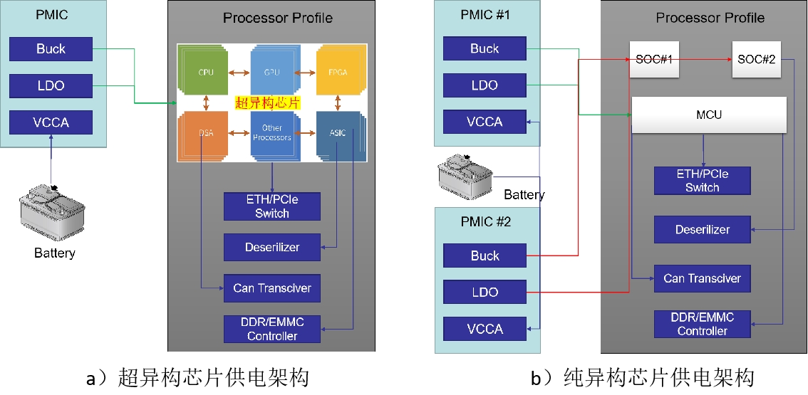
In terms of domain control architecture design, hyper heterogenous chips usually centralize all computing resources onto a single chip, which also drives and controls the power supply of all related chips, such as serializers, switches, Can transceivers, and camera control ends, through a series of control connections. Therefore, we usually refer to this control connection as a series control, and the power control chain is usually uniformly managed by the unified PMIC of the central chip. Of course, considering the low power consumption characteristics of the architecture, the PMIC of the central chip may also be split into master-slave control, where the main road realizes power control management under full power consumption, and the auxiliary road realizes separate power management when there is a demand for reducing power consumption (such as activating only the internal MCU module through the PMIC link).
In contrast, for pure heterogenous chip ADAS domain control architecture, the power tree design usually follows the single chip single control approach. For example, if MCU, SOC, and GPU are integrated into the same system architecture, a separate power control approach is usually adopted, and each chip’s power supply is individually controlled, while chips like serializers and CAN transceivers rely on a customized power control module for their power on and off control. For instance, dedicated power control can be implemented on the wake-up of CAN, or on the bypass of image output control. For chips like Switch, they can be controlled by MCU to turn on and off separately.## Design of Basic Power Tree for Intelligent Driving System
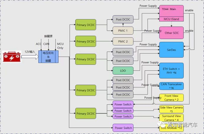
The following diagram illustrates the power structure of the intelligent driving system that will be elaborated in detail in this article. The entire front-end power supply of the tree is provided by the vehicle’s power battery. Considering the enormous power consumption of the intelligent driving system, the power supply is usually provided in high-voltage mode by a large battery. Of course, in certain special situations, it can also be switched to a small battery supply (such as the sentinel mode started by the lower power in a certain time, or the long endurance mode activated by new energy vehicles in the later stages of driving). Additionally, there are different ways to wake up the power supply (such as directly starting the IG ON by ACC mode, injecting CAN network wake-up messages, or other mechanisms that require separate chip wake-up operations).
The entire power-on management process involves the initial DCDC buck conversion, which is generally used to convert the 12V battery voltage into lower voltage values such as 5V, 3.3V according to the demand for different chips. For example, TDA4 requires 3.3V power supply, and other chips require 5V power supply. After connecting to the PMIC power management module for initial voltage regulation, the main operation chip of the intelligent driving system can be directly powered through voltage distribution control. Of course, there are also some chips (such as serializer/deserializer 1.0V-1.8V, CAN transceiver 5V, Ethernet Switch1.0V-3.3V, etc.) that require secondary voltage conversion processing Post DCDC after initial buck configuration according to their own requirements.
In addition, since there is a mutual dependence between the startup and data processing of the intelligent driving system, the central processing chip SOC/MCU is usually considered as the enabling terminal for other chips. For example, if the SOC is used for processing the data of visual perception input source, a control connection line (such as IIC line) needs to be set between SOC and serializer/deserializer, and between SOC and the power switch directly connected to the camera as an enabling line adjustment. In addition, if MCU is used as the data processing terminal for millimeter wave radar (trajectory planning), its control of the input and processing of the millimeter wave radar data is the central task. The enabling and power control of the corresponding CAN transceiver can be directly controlled by the vehicle’s control MCU, or it can be directly connected to the vehicle’s constant power supply.
 During the whole power tree design process, design work including reverse voltage design, wakeup response design, voltage stabilization design / voltage transformation design (DCDC, LDO, PMIC), and power switch design is needed. Here are several typical chip selection and corresponding feature parameter explanations:
1) LDO (MPQ20051): low dropout linear regulator, which can provide up to 1A current and 140mV voltage. Its adjustable output voltage range is from 0.8V to 5V when the input voltage is from 2.5V to 5.5V. Internal PMOS transfer element allows low ground current from 130uA, making MPQ20051 suitable for battery-powered devices. Other features include low power shutdown, short circuit and thermal protection.
2) DCDC (MAX20074ATBA/V+): represents the sync buck regulator IC. It is the lowest automotive synchronous buck controller with only 3.5uA static current in light load.
3) DCDC (MPQ2166): is an internally compensated, dual-channel, PWM, synchronous, buck regulator that works under input voltage from 2.7V to 6V, and produces an output voltage as low as 0.6V. MPQ2166 can be configured as a 2A/2A or 3A/1A output current regulator, with a static current as low as 60µA. MPQ2166 has a peak current mode control and internal compensation, and is capable of low dropout configuration. Both channels can run with 100% duty cycle, and full protection features include per-cycle current limit and thermal shutdown.
4) PowerSwitch (MAX20086–MAX20089): a dual-channel/four-channel camera power protector IC that provides up to 600mA load current for each channel among its four output channels.
As for PMIC chips, the following several types are mainly used here to achieve different power management control:
5) PMIC (PF71): is an integrated circuit for power management designed specifically for high-performance i.MX 8 processors. It has five high-efficiency step-down converters and two linear regulators, which are used to power the processor, memory, and other peripherals. Built-in one-time programmable memory stores critical startup configurations, greatly reducing the external components usually used to set output voltage and external regulator order. Stabilizer parameters can be adjusted after startup via high-speed I2C to provide flexibility for different system states.6) PMIC (TPS6594-Q1): TPS6594-Q1 is a power management chip IC with 5 BUCK and 4 LDO, which is particularly suitable for intelligent driving safety-related automotive applications in the industry. The device can provide four flexible multi-phase configurable BUCK voltage regulators with 3.5A output for each phase, and an additional BUCK voltage regulator with 2A output. Each output is individually protected against battery shorts, ground shorts, and overcurrent situations. These ICs operate from 3V to 5.5V power supply and 3V to 15V camera power supply, and the input to output voltage drop is only 110mV (typical) at 300mA.
7) Primary DCDC (MAX20098): This is an automotive-grade 2.2MHz synchronous step-down controller IC with 3.5μA IQ. This IC is powered from input voltages of 3.5V to 42V, and can operate at 99% duty cycle under voltage drop conditions. This type of operation is suitable for applications requiring medium to high power and operating in a wide input voltage range, such as providing necessary voltage under cold engine start or engine stop start conditions. The IC also provides a time-sync output signal SYNC, enabling two controllers to run in parallel. The FSYNC input programmability supports three frequency modes to optimize performance: forced fixed frequency operation, skip mode with ultra-low standby current, and synchronization with external clock. When used with the programmable spread spectrum option for frequency modulation, this IC can minimize EMI interference.
Example-based Power Network Management
This article provides a detailed explanation of how a dual PMIC (TPS6594-Q1) power can be connected to typical processors and other peripheral components for effective support of Power Distribution Network (PDN). The PDN power network management module can achieve board-level isolation of the main microprocessor (MCU) and the rest of the high computing power chip voltage resources according to the power requirements of its processor. Utilizing this board level power isolation achieves an ideal product functional architecture.
The design of the entire PDN distribution network mainly includes the following:① PDN Power Connection
② PDN Digital Control Connection
③ Main and Auxiliary PMIC Default Internal Module Management NVM Content
④ PMIC Sorting Settings to Support Different PDN Power State Transitions for Advanced Processors
The system PMIC data processing requires a description of recommended operations, electrical characteristics, external components, packaging details, register mappings, and overall component functions. The PMIC (TPS6594-Q1) device has different orderable part numbers (PN) with unique NVM settings to support different end-product use cases and processor types. Each PMIC’s unique NVM settings are optimized for each PDN design to support different processors, process loads, SDRAM types, system function security levels, and end-product characteristics (such as low-power modes, processor voltages, and memory subsystems). NVM settings can be identified by module ID number NVMID and module register NVMREV. Each PMIC device can be distinguished by part number, NVMID, and NVMREV value.
The figure below shows the power mapping between dual TPS6594-Q1 PMIC power management and processors, supporting voltage domains for independent MCUs and main power rails.
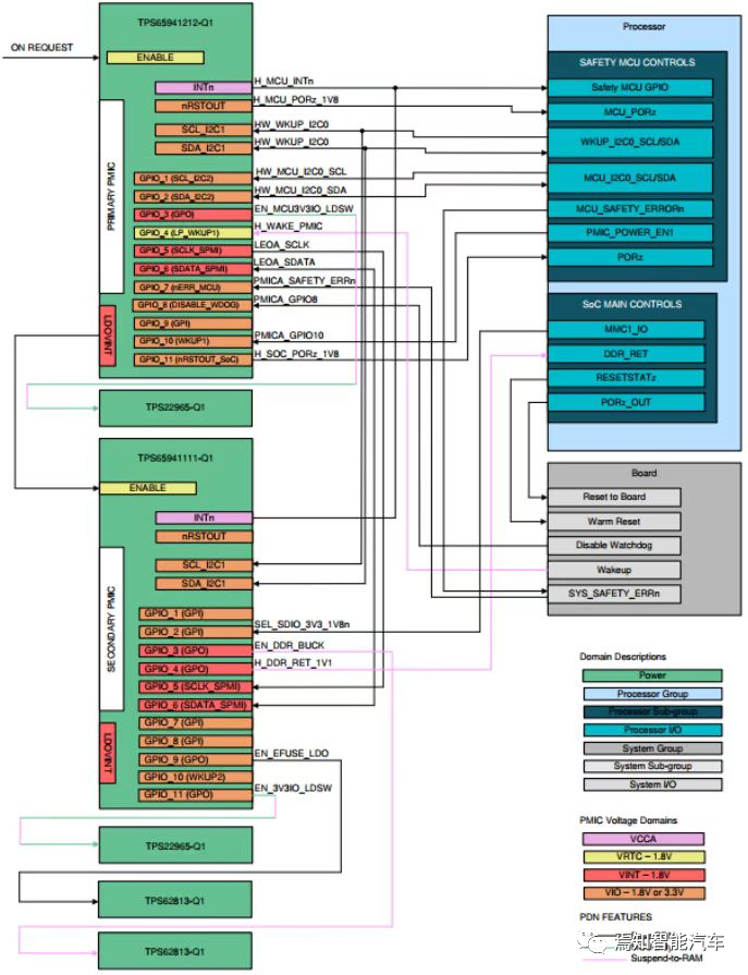
As shown in the figure above, there needs to be a series external power FET between the PDN input power and the PMIC. PMIC achieves voltage monitoring before and after FET through OVPGDRV pin, and when an overvoltage event greater than 6V is detected, FET can quickly isolate PMIC from the input power to protect the system from damage. This includes all power rail MOSFET output signals, and any upstream power connected to the FET is not protected from overvoltage events. The load switches for MCU and major I/O domain power supply, the discrete buck power supply for DDR, and the separate voltage regulator LDO for EFUSE power supply are all connected to FET in order to extend the overvoltage protection capability for these processor domains and discrete power supplies.In addition, there are several corresponding parameter settings included in the internal structure of the entire power management module as shown in the above figure.
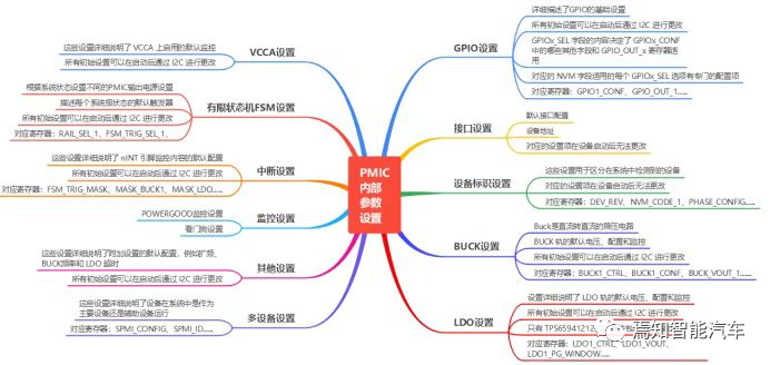
In the above configuration, two PMICs use a 3.3V input voltage. For functional safety applications, a protection FET is connected to the OVPGDRV pin of the main PMIC before VCCA, allowing the input voltage of the PMIC to be monitored. The VCCA voltage must be the first voltage applied to the PMIC device, and the PMIC’s VIOIN is powered by the corresponding PDN through the load switch after VCCA. The load switch also provides the voltage source of VDDSHVxMCU processor. By introducing the PMIC GPIO control signal of VIO_IN, it can ensure that the active state can be maintained during MCU Only low-power mode and be disabled during data saving (also known as suspend to RAM) period in DDR to reduce PMIC power consumption.
For the dual-voltage I/O situation, support is needed for both 3.3V and 1.8V. Using a processing terminal LDO with a logical high-level default value, the initial voltage I/O value can be set to 3.3V through GPIO control signals. During the power-on period of the processor, the bootloader SW can set the GPIO signal to a low level to ensure that the user can select the appropriate voltage (1.8V) as needed. At the same time, PMIC can control the LDO1 voltage processor to establish I2C communication with PMIC during the operation system start-up.
Here we can give an example of how MCU Only control logic is implemented for some heterogenous chips. For example, in TDA4 chip MCU Only mode control, it is necessary to use four discrete power components in the power distribution network PDN, three of which are required, and one is optional, depending on the characteristics of the final product. Two TPS22965-Q1 load switches connect the VCCA_3V3 power rail to the power protection processor I/O domain. Normally, two load switches are required to achieve isolation between calculation domain NPU and real-time domain MCU, and each module is controlled separately. Of course, power isolation can also be established between the main processors of the MCU Only low-power operation. TPS62813-Q1 buck converter can also provide the required power voltage (1.1V) for the storage unit LPDDR4 SDRAM module.From the TPS6594-Q1 device to other connections of the processor, the GPIO lines can be used to provide error monitoring, processor reset, processor wake-up, and system low-power mode through signals. Specific GPIO pins need to be assigned to specific key signals to ensure proper operation in low-power mode with only a few GPIO pins.
This article is a translation by ChatGPT of a Chinese report from 42HOW. If you have any questions about it, please email bd@42how.com.