
Author | Jessie
NVIDIA DRIVE AGX is an expandable and open autonomous driving car computing platform, serving as the brain of the autonomous driving car. As a first-class hardware platform among similar products, NVIDIA DRIVE AGX provides high-performance and energy-efficient computing for functional safety of artificial intelligence autonomous driving. In terms of hardware, NVIDIA DRIVE embedded supercomputing platform processes data from cameras, common radar, and lidar sensors to perceive the surrounding environment, determine the car’s location on the map, and then plan and execute a safe driving route. In terms of software, NVIDIA DRIVE AGX has scalable and software-defined features, allowing the platform to provide advanced performance to help autonomous driving vehicles process large amounts of sensor data and make real-time driving decisions. The open NVIDIA DRIVE software stack also helps developers use redundant and diverse deep neural networks (DNNs) to build perception, mapping, planning, and driver monitoring functions. Through continuous iteration and wireless updates, this platform is becoming increasingly powerful. At the same time, the open NVIDIA DRIVE SDK provides all the building blocks and algorithm stacks needed for developers to build and deploy various advanced autonomous driving applications, including perception, positioning and map drawing, planning and control, driver monitoring, and natural language processing. This article will be divided into several sections to take Orin-x, the most widely used mainstream NVIDIA chip, as an example and explain how to conduct development and application from software to hardware levels in two directions.
NVIDIA Internal Architecture Design
Taking Orin-x as an example, the CPU includes a main CPU complex based on Arm Cortex-A78AE, providing general high-speed computing capability; and a functional safety island (FSI) based on Arm Cortex-R52, providing isolated on-chip computing resources, reducing the need for external ASIL D functional safety CPU processing.
The GPU is NVIDIA Ampere GPU, providing advanced parallel processing capabilities for the CUDA language, and supporting multiple tools, such as TensorRT, a deep learning inference optimizer and runtime that provides low latency and high throughput. Ampere also provides state-of-the-art graphics capabilities, including real-time ray tracing. Domain-specific hardware accelerators (DSAs) are a set of dedicated hardware engines designed to offload various computational tasks from the computing engine and perform these tasks with high throughput and high energy efficiency.The high-level architecture of SoC is shown in the following figure, which is divided into three main processing complexes: CPU, GPU, and hardware accelerator.
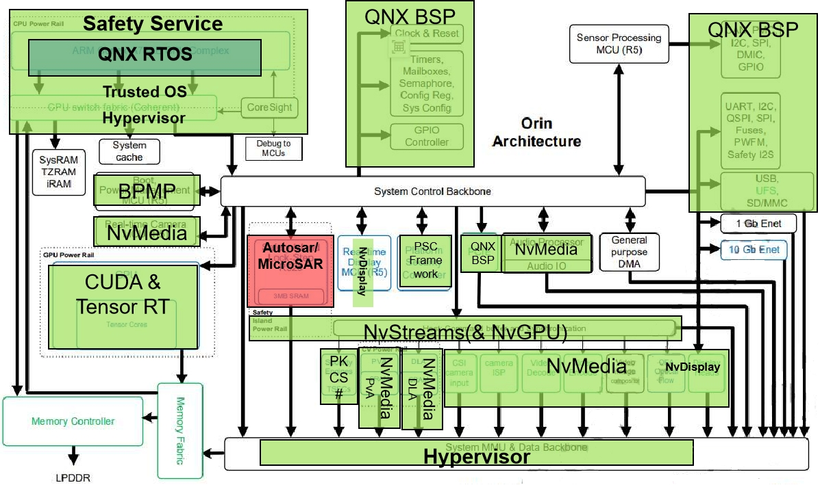
The overall internal architecture of the chip is mainly designed according to functional blocks. It includes QNX BSP (Clock source & System restart, CAN/SPI/I2C/GPIO/UART controller, Configuration register, System configuration) for operating system, real-time operating system QNX RTOS, Nv multimedia processing module (Sensor processing module MCU (R5), PVA, DLA, Audio Processor, MCU R5 configuration real-time camera input), Classic Autosar processing module (used for Safety Island Lock-Step R52s), Safety Service (ARM Cotex-A78AE CPU Complex, CPU Switch fabric Coherent, Information security PSC), and neural network processing module (CUDA & TensorRT).
Typical architecture design of autopilots based on Nvidia chips
Conventional SOC system architectures are typically designed with SOC+MCU dual- or even triple-chip configurations. Due to its superior computing performance, SOC generally performs better than MCU in compute-intensive applications such as perception and planning.
MCUs have higher functional safety levels and can be used as verification output for control execution. The industry has been mixed in its opinion on whether Nvidia chips can independently undertake tasks as a super-heterogeneous chip similar to TDA4. In principle, Nvidia chip designs, from both the Xavier and Orin series, have rich AI and CPU computing capabilities. This kind of capability is fully adaptable to the entire solution design for developing level 2+ autonomous driving systems.Then, has the industry advocated such design solutions? The answer is no.
Regarding the latest safety requirements in the Nvidia Datasheet, the recommended architecture design for the Orin chip still requires the use of a specific MCU for failure analysis and risk assessment. This can quickly locate serious faults in the system to ensure compliance with the automated driving safety integrity performance requirements defined by the ISO 26262 standard (this will be explained separately later). Additionally, due to the entire domain controller’s power management, integrating an external MCU can also enhance its power management capabilities, including entering and exiting sleep modes, and more.
The MCU designed above can also be called the Safe MCU (SMCU) to some extent. During the system development process, some high-security MCU (generally needs to achieve ASIL D level) are required, such as the Infineon Aurix TC series and the Renesas RH850 series, which can act as MCUs to access Orin’s SMCU. SMCU can actually act as a power control and a serious failure prevention for the entire system’s development.
As shown in the figure above, the three-layer failure safety framework based on the Nvidia chip’s design system architecture is represented. Overall, the structure achieves three-level failure safety protection from the basic services, operating system, virtual machine, and implementation runtime environment at the SOC level to the real-time operating environment of the MCU. SOC and MCU layers perform healthy and independent watchdog monitoring at the NvIVC, NvIPC, SPI/Error Pin level. Internally, SOC itself will carry some lockstep safety verification Lockstep FSI and run the hypervisor on the Carmel CPU complex running the capture stack and applications. The CPU core uses a high-function security level QNX operating system, for application software watchdog, middleware, application layer software, and driver software resource scheduling. Of course, for real-time operating systems, it still runs on the standard Autosar.The security architecture shown in the figure below illustrates how the external MCU supports the boot data stream on the SOC and performs effective secure boot through a standard error report/propagation data stream. The entire program and data boot loading process includes three levels: Boot L1 level CCPLEX, Boot L2 level FSI, and Boot L3 level External MCU.
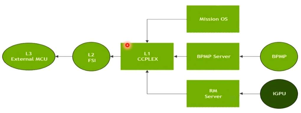
During the L1 level program boot process, the bottom-level boot includes loading the bottom-level boot program to the BPMP server using the “Boot and Power Management Processor (BPMP)” terminal (a small ARM core located at the core position of the system), and the corresponding boot program file is called by virtual machine hypervisor or operating system Safety OS. Overall, Cortex-R5 of BPMP can achieve:
-
Lockstep core pairing
-
Arm 7-R ISA
-
Vector interrupt support: based on the Daisy Chain Arm PL192 Vector Interrupt Controller (AVIC)
-
TCM interface for local SRAM
-
Complete instruction and data cache (involving 32KB instruction cache I-Cache and 32KB data cache D-Cache)
-
Arm processor correction
At the same time, the bottom-layer iGPU core is also driven by the RM integrated server. Finally, the operating system task scheduling, boot management program loading, and RM server drive GPU core of the professional tasks are completed in the first layer to load the boot program L1 CCPLEX (called CPU Complex, which is a high-performance 64-bit Arm core in NVIDIA).
In addition, the L2 level mainly involves the functional safety island verification FSI mentioned in the previous article. It will be explained separately in subsequent articles.
Finally, the external SMCU can also do an extra layer of security protection and boot management configuration. This can drive the entire chip from a security perspective.## Design principles of functional safety island
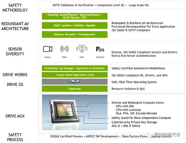
Figure 2 shows how to load the FSI and underlying module driver bootstrap program in the NVIDIA series chips. In terms of functional safety design, the NVIDIA series chips achieve ASIL D system capability design and ASIL B/D random error management capability design by setting targets. This includes SOC chip hardware-based ASIL decomposition requirements to each core, ensuring that inter-core design consistency can meet ASIL D requirements, and applying standard ASIL D development processes to the entire functional safety design. We conduct corresponding safety designs for safety process, Drive AGX, operating system Drive OS, Drive Work, sensors, redundant architecture design, and safety strategies from the bottom up.
The Functional Safety Island (FSI) of the NVIDIA series chips is a core that contains a Cortex-R52 and Cortex-R5F real processor cluster and a time processor with a dedicated I/O controller. For example, the FSI module in Orin-X has its own voltage rails, oscillators, PLL, and SRAM to ensure minimal interactions with other modules inside the SOC and no interference between the above modules.
The FSI functionality of the Orin-x series includes:
Cortex-R52 processor, also known as the secure CPU, has 4 cores under DCLS (dual-core lock-step) mode (a total of 8 physical cores) and can run the classic AUTOSAR operating system. It achieves error handling, system fault handling, and other customer workload with a comprehensive performance of about 10KDMIPs.
Cortex-R5F processor, also known as the encryption hardware security module (CHSM), is used to run encryption and security use cases, such as secure vehicular communication (SecOC) through the CAN interface.
The overall FSI mechanism includes some security instructions and control interface information:
-
The tight coupling memory, instruction, and data cache of each core of the security and CHSM CPU.2. The total on-chip RAM on the secure island is 5MB to ensure that code execution and data storage remain within FSI.
-
There are dedicated I/O interfaces on the island for communication with external components, including 1 UART and 4 GPIO pins.
-
Hardware security mechanisms, such as DLS, CRC, ECC, parity check, and timeouts, are implemented on all IPs within FSI. There are also dedicated thermal, voltage, and frequency monitors.
-
Logic isolation is implemented to ensure sufficient error recovery time for other parts of the SoC in the event of an error in FFI.
FSI Instance Analysis 1:
In this article, we will use an example to illustrate the corresponding error handling mechanism designed for FSI, including the handling mode for the following processes:
-
Various methods for debugging CSI capture errors on the Xavier-based platform.
-
How to determine which method to use for debugging.
-
How to identify errors.
-
Possible root causes of errors.
The layers in which errors may occur during the camera capture process are as follows:
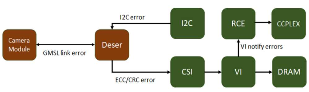
Whenever the VI hardware engine encounters an error when decoding CSI data packets received at the SoC CSI interface and writing raw frame data into memory, it notifies RCE of these errors. The capture stack running on CCPLEX can query the capture status from RCE and display the ID of the CSI data stream, the VC ID where the error occurred, the error type, and detailed errors for each error type. The error status provides a good starting point for identifying the root cause and determining the subsequent steps. If the VI engine fails to capture frames successfully without encountering errors and reporting them to RCE, a frame start or end timeout error message prompt will be displayed.
This may be due to one of the following two reasons:
-
The deserializer is not receiving streaming data.
-
The VI channel is not configured to capture the correct data type/VC id.
How does NVIDIA consider information security for its chipsets?For NVIDIA chips, there are two levels to effectively ensure information security: one is the Tegra secure kernel module inside the information security chip. Although this chip once had security vulnerabilities in 2018, in which an extreme hacker exploited the vulnerability in the NVIDIA Tegra X1 chip to crack the Switch host, this loophole allowed anyone to run arbitrary code on it, meaning that homemade systems and pirated software could be run freely. However, through continuous internal optimization, NVIDIA has largely completed the patching of vulnerabilities.
For example, in the original Nintendo Switch console using the same Tegra X1 CPU, a vulnerability was found in the ROM boot loader and was repaired by recovery mode and buffer overflow. NVIDIA can use built-in programmable fuses to store patches in internal ROM to solve such repair problems. This reduces code bugs by considering weak links and taking security into account.
Moreover, the nature of hardware design means that some internal hardware modules cannot be accessed by CCPLEX, and only BPMP can manipulate them. All low-level boot steps, including u-boot, can be secured by signed binary files. Their keys can be stored in one-time programmable fuses in CPU. U-boot itself can be configured to use signed FIT images, providing a secure boot chain all the way to the Linux kernel. The initial ROM boot loader and TegraBoot also support fully redundant boot paths.
Tegra is a unique information security chip kernel in NVIDIA chips, and Tegra Security Controller (TESC) is an information security subsystem that has its own trusted root ROM, IMEM, DMEM, Crypto accelerator (AES, SHA, RNG, PKA), critical links, and critical storage. TSEC provides an on-chip TEE (Trusted Execution Environment) that can run NVIDIA-marked processing code. TSEC is a typical security video playback solution, downloading HDCP1.x and 2.x connection authorizations and complete cable link detection required for information security operations.Overall, TSEC provides support for:
1) HDCP 1.4 on Line-side HDMI 1.4 and HDCP 2.0 2.1 on Line-side HDMI 2.3;
HDCP link management does not expose protected content, nor does it require a software key running on the CPU. There are two software programmable independent instruction queues (up to 16 instructions) for HDCP link management; the entire chip can disable HDMI output independently of the player when HDCP status check fails.
2) Platform Security Controller;
It is a high-security sub-system that can protect and manage assets (keys, fuses, functions, and features) within the SOC and provide trusted services to enhance the SOC’s ability to resist attacks and protect against software and hardware attacks on the subsystem itself.
3) Key Management and Protection;
PSC will be the mechanism that has access to the most critical keys in the chip. This sub-system represents the highest level of protection within Orin-x and has a high degree of resilience to various software and hardware attacks.
4) Trusted Services;
For example, during SOC secure boot, primary PSC services can perform effective secure identity authentication, provide additional keys/IDs/data, key access and management, random number generation, and trusted time reporting.
5) Information Security Monitoring.
PSC will be responsible for regular security management tasks, including continuous assessments of SOC security status, proactive monitoring for known or potential attack patterns (such as voltage faults or thermal attacks), reducing hardware attack risks, and taking effective actions when attacks are detected. PSC will be able to accept various software updates as solutions to improve the robustness of on-site systems.
Secondly, the application of the Security Engine (SE) is discussed. It provides hardware acceleration for cryptographic algorithms.
There are two scenarios where the Security Engine SE is useful for software. One is that TZ-SE can only be accessed by trusted software in the trusted zone. The second is that NS/TZ-SE can be configured to be accessed by trusted software zones or non-secure software. The Security Engine SE can provide hardware acceleration and hardware-supported key protection for various encryption algorithms. The encryption algorithms provided by SE can be used by software to establish encryption protocols and security features. All encryption operations are based on encryption algorithms approved by the National Institute of Standards and Technology (NIST) international standard technology association.The security engine SE from NVIDIA can support all of the following information security capabilities that comply with NIST: symmetric and asymmetric encryption and hash algorithms, side-channel countermeasures (AES/RSA/ECC), independent parallel channels, hardware key access control (KAC) (based on rules, enhanced hardware access control for symmetric keys), 16xAES, 4xRSA/ECC key slots, hardware key isolation (only for AES key slots), read protection (only for AES key slots), hardware key slot functions, key wrapping/unwrapping functions (AES -> AES key slots), key separation from key slots (KDF -> AES key slots), and random key generation (RNG -> AES key slots).
Summary
This article presents a comprehensive analysis of the core architecture, functional safety, and information security features and advantages of NVIDIA chips from various aspects. It is particularly important to consider its internal architecture and its functional and information security capabilities when using the NVIDIA chip series for development and tuning. Subsequent articles will provide detailed strategy analysis from the perspectives of hardware and software development.
This article is a translation by ChatGPT of a Chinese report from 42HOW. If you have any questions about it, please email bd@42how.com.