Author |
Shawn Ouyang, System Architecture Engineer at Xilinx R&D center, UK;
Dr. Andrew, Fellow at Xilinx Research Center, UK
Introduction
FPGA is a device for implementing programmable digital logic. Like CPU, GPU/NPU and specialized ASIC circuits, FPGA is now also widely used in the implementation of neural networks (NN).
Today, Xilinx and Intel are the two leading FPGA manufacturers in the world. In addition to these, there are several smaller manufacturers, including Microchip, Lattice Semiconductor and GOWIN Semiconductors.
The programmable configuration of FPGA includes programmable logic blocks and programmable interconnects. In addition to programmable configuration circuits, FPGA can also include “hard” blocks that are not configurable, such as CPUs, I/O peripherals and AI tensor blocks.
So what makes FPGA particularly suitable for implementing neural networks compared to other platforms? Let us first compare NN’s FPGA implementation with GPU / NPU and ASIC implementations, without considering the general but relatively slow CPU.
It turns out that FPGA’s unique advantage lies in its reconfigurability. This also explains why many academic resources are currently researching how to use FPGA efficiently for NN implementation: because of its programmability, FPGA is the only platform that allows researchers to try and demonstrate (other than simulation) their new neural network hardware implementations.
If the running algorithm and model are determined, and the shipment scale for commercial use is large enough to dilute the one-time R&D and chip-making costs, ASIC will be the preferred choice, because compared with FPGA, ASIC is expensive, slower and relatively higher in power consumption. However, in many current application scenarios such as autonomous driving, the neural network algorithm used is uncertain, and the manufacturing process often requires very high standards, so the one-time R&D and chip-making costs are very high, and using ASIC is not the most cost-effective option.
After optimizing for the same NN on FPGA, the speed can be close to that of high-end GPUs, but it requires more engineering effort. Therefore, in the early stages of NN model exploration, to quickly try out NN models, using high-end, state-of-the-art FPGA is more efficient than using general-purpose GPU or NPU.Using FPGA rather than ASIC and GPU has unique advantages in the following applications:
- Prototype design and testing of digital logic for ASIC development
- Demonstration of some of the latest research algorithms by building custom digital integrated circuits using FPGA
- Use of FPGA for small to medium volume and high-value commercial applications when no equivalent ASIC is available, or hardware needs to be reconfigured
Unlike real-time processing that is required for ensuring interoperability in applications such as wired or wireless communications, FPGA implementations of image processing neural networks typically do not need to meet clock speed requirements. The maximum frame rate that can be processed per second is limited by the fastest clock frequency achieved through logic synthesis, which is typically slower than that of GPU or ASIC. However, even with a slower clock frequency, the functional consistency can still be maintained, which can validate the logic of the circuit.
Below, this article qualitatively compares FPGA with ASIC/GPU NN implementations. It is usually difficult to make equal comparisons between different hardware, since the ultimate performance outcome depends not only on the implementation method but also on the specific device used. Furthermore, the fast development of GPU and FPGA technologies and the continuous emergence of new generations of devices also constantly change the competitive landscape.
Why Choose FPGA?
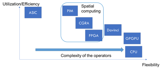
Shown in the figure is an example of the hardware architecture of a neural network implementation. GPU is a highly flexible general-purpose hardware, but its utilization/efficiency is relatively low, while ASIC can achieve extremely high efficiency and integration of specific algorithms but lacks flexibility and can only support a limited range of algorithms.
FPGA, on the other hand, falls between GPU and ASIC. FPGA does not “beat” GPU and ASIC in all indicators of neural network implementation, but in some respects, FPGA has unique advantages, such as high efficiency and flexibility. These features allow FPGA to support a large number of acceleration methods, such as quantization, sparsity, and data pipeline optimization.
In summary, for rapidly developing neural network algorithms, FPGA will be the best platform for ASIC digital logic prototype design and testing, technology demonstration.
 ### 2.1 Comparison between FPGA and ASIC for Neural Network Implementation
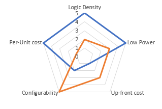
Compared to ASIC, FPGA with the same logic function characteristics at the same process node is slower, consumes more power, and has a higher unit cost. However, this is a necessary cost to be paid in exchange for FPGA configurability.
ASIC design and production require a long time and are expensive, while FPGAs can be directly acquired. Therefore, in small and medium-sized batches and high-value applications, FPGA is preferred over ASIC because they can meet the required capacity and I/O functions, especially in cases where hardware requires flexible reconfiguration.
An example of such an application is SmartNIC, for which Xilinx and Intel both provide dedicated products for AI scenarios.
Since ASIC hardware cannot be reconfigured like FPGA, it is preferable to use an NPU that can perform different models flexibly rather than a hard-coded and optimized NPU for a specific model in ASIC.
In ASIC, digital hardware modules that accelerate specific NN operators can be used with a general-purpose NPU. Although the architectures of these modules are fixed, they can still be configured to some extent : for example, they can accept different weights or execute one of the supported operators at any given time.
2.2 Comparison between FPGA and GPU/NPU for NN Implementation
GPUs and NPUs typically have a set of general purpose processing units (tensor cores), and NNs are deployed and executed on PEs with dedicated compilers.
For models specifically optimized for FPGA, FPGA may be more energy-efficient than GPU because it can design dedicated logic blocks to use fine-grained quantization to reduce the amount of computation for specific models while maintaining accuracy, whereas GPU/NPU only supports limited quantization methods.!Figure 3: Some FPGAs include tensor cores such as GPUs, as well as programmable “soft” logic [2]
![Figure 3: Some FPGAs include tensor cores such as GPUs, as well as programmable “soft” logic [2]](https://42how-com.oss-cn-beijing.aliyuncs.com/article/image_20230103201128.png)
Modern GPU cards have a large amount of very fast memory (e.g. installed with GDDR), while FPGAs have relatively little on-chip memory (e.g. “BlockRAM” in Xilinx devices). To store model weights, FPGA implementations typically use external DDR SDRAM. Generally, the external memory used in FPGA implementations has a slower access rate than the internal memory used in GPUs.
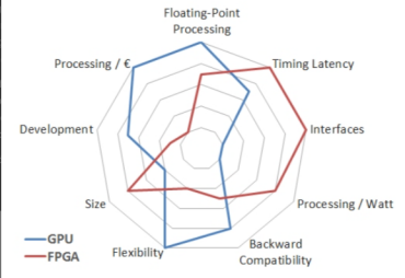
Even Intel and Xilinx admit that FPGAs are not better than GPUs in terms of all performance indicators. However, Intel also points out that compared to GPUs, FPGAs have advantages in low latency, hardware customization, interface flexibility, and power consumption. An objective evaluation by Berten DSP also gave similar conclusions as shown in the figure below.
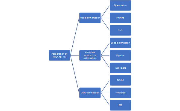
NN Model Optimization Techniques for FPGAs
Reference [3] analyzed optimization techniques that can be used to prepare neural networks for FPGA (or ASIC) implementations:
- Model Compression
- Weight Quantization
- Quantization can be as low as 1-2 bits with limited accuracy loss.
- Weight Pruning
- If pruning is considered during training, the accuracy loss caused by pruning is reduced.
- Matrix Factorization SVD
Reduce the number of weights and multiplications by lowering the matrix rank through singular value decomposition (SVD) when using matrix multiplication.
- Hardware Architecture Optimization
-
Loop Optimization
-
Data Flow
-
Inter-layer Fusion
- Convolution implementations that reduce complexity, such as FFT and Winograd methods.
3.1 FPGA used for CNN network acceleration
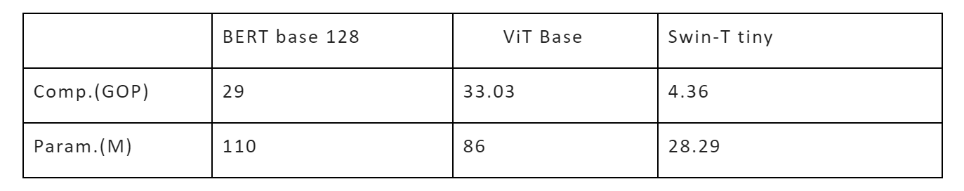
Table 1 lists the parameter scale and computational complexity of several typical CNN-based neural networks.
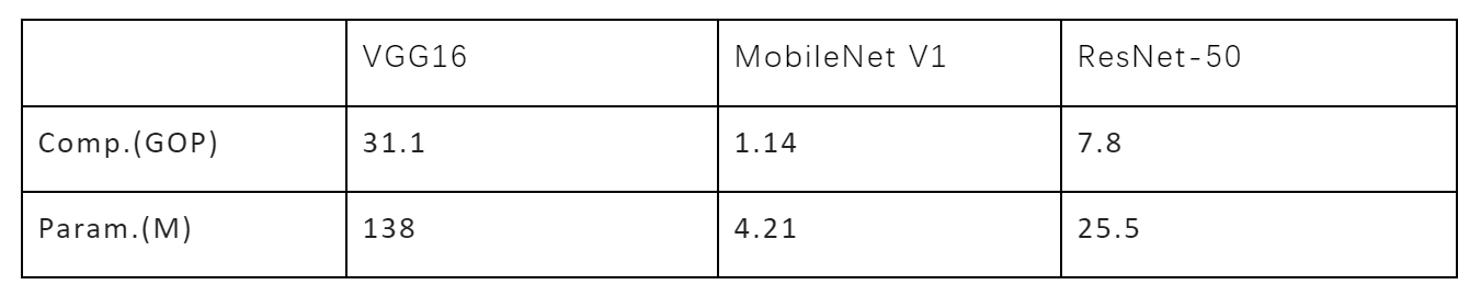
Based on the typical neural networks listed in Table 1, multiple FPGA implementation schemes specifically for CNN networks were collected.
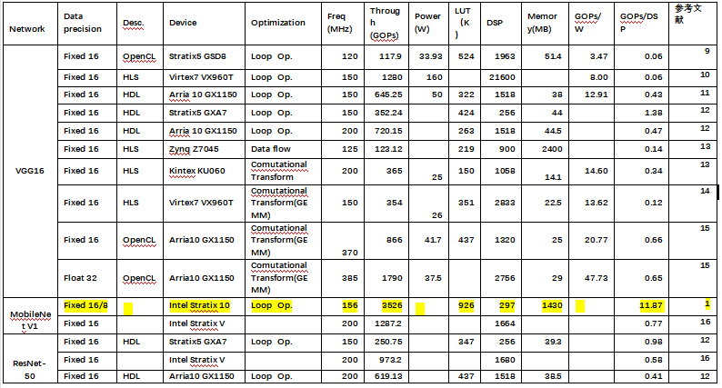
From Table 2, we can see that literature [1] achieved the highest computational efficiency among all known papers on CNN, improving the throughput and latency by 2-4 times compared with other nearest FPGA implementation schemes. The implementation also achieved 3000FPS inference speed on the ImageNet dataset. The main reason is that by using the flattened streaming hardware architecture on FPGA and the soft-hard co-design of multi-precision mixed quantization, the size and computational complexity of the model were greatly reduced.
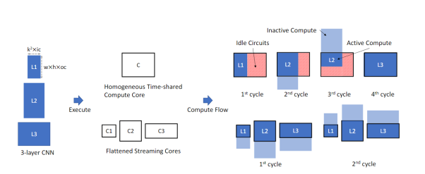
Most of the current CNN accelerators, including NPUs, use a homogeneous large-scale pulse array. With this architecture, multiple images can be processed in parallel in different PEs or PE sets. NN layers can be sequentially processed by reusing identical hardware, each layer having different configuration/weight. For example, NVIDIA GPU includes “tensor cores”. In addition, Xilinx and Intel provide FPGAs with dedicated AI modules that can be used to implement a PE array. The complexity of each PE can be adjusted: a low-complexity PE may only contain one set of multiplication/adders, while a higher-complexity PE may be a small instruction-set programmable processor. As many different convolutional layers reuse the same hardware computing unit, the pulse PE array is time-division multiplexed. However, different convolutional layers’ input data size, channel number, convolution kernel size, and emerging convolution structures such as depthwise all make it increasingly difficult to achieve efficient implementation on a single large computational core.
Therefore, another hardware architecture is used in the literature [1], which breaks down the CNN network layer by layer and streams it to different computing units in a pipeline manner. Each computing unit is activation value-driven.

As shown in the following figure, there are three different convolutional layers (L1, L2, L3) implemented on the isomorphic pulsating array and flattened architecture in different ways. Under the isomorphic pulsating array architecture, a large PE array computing unit C is used, while the flattened architecture uses three smaller computing units C1, C2, and C3. Since the size of the three convolutional layers is different, using a single large isomorphic array structure will cause idle parts in the computing unit, resulting in low hardware utilization. The flattened architecture has multiple computing units of different sizes to adapt to the size of each convolutional layer, thus fully utilizing hardware resources. As shown in the figure below, the isomorphic array architecture requires 4 cycles to complete the calculation of the 3 convolutional layers, while the flattened architecture only requires 2 cycles.
Based on the flattened architecture design, combined with mixed-precision quantization and more logical units of FPGA, or even multi-FPGA cascading, the author proposes an automated tool framework that can map the complete CNN network to FPGAs. The framework first uses self-developed algorithms to perform fixed-point quantization and offset search for pre-trained CNN models at multiple precisions, thereby generating an optimized model that can meet accuracy requirements after quantization. Also, since the flattened architecture consists of multiple computing units, each computing unit can be quantified with different bandwidth precisions to ensure minimizing accuracy losses while compressing model computation. In the above stages, the framework also accurately estimates hardware resources, including delay, LUT, and BRAM utilization, etc. After generating a systemVerilog according to the optimized model and resource estimation based on the prepared verilog library, the framework synthesizes and generates FPGA hardware files.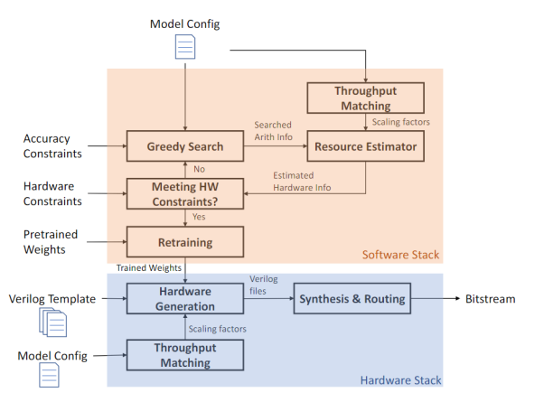
3.2 FPGA for Transformer Network Acceleration
Table 3 lists the parameter size and computational complexity of several typical neural networks based on Transformer.
Various FPGA implementation solutions for Transformer networks have been collected for several typical neural networks listed in Table 3.
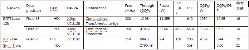
Among the implementation solutions in Table 4, the one achieved in reference [18] has the highest power efficiency, which mainly optimizes the attention module and the feed-forward network (FFN), also called a multilayer perceptron (MLP), in Transformer networks.
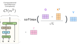
The typical expression of self-attention formula in Transformer networks is shown in the following figure. For matrix multiplication in the self-attention module, if the sequence length is n, the time complexity is O(n^2), which will also consume N^2 time and storage.
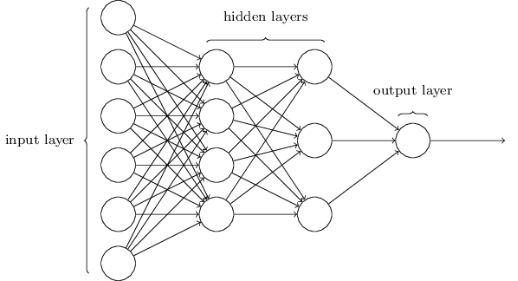
 The structure diagram of the feedforward neural network (FFN) is shown below, consisting of input layer, hidden layer, and output layer. Each layer has several neurons, so a weight matrix is defined for each layer. The specific calculation details are not discussed here. The key point is that the calculation between each layer is essentially a matrix vector multiplication.
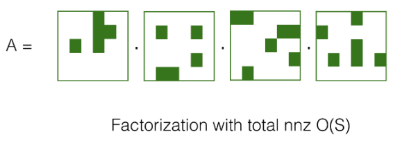
In both the attention and FFN modules, there are matrix-matrix multiplication and matrix-vector multiplication calculations. Sparsely decomposing the matrix is an effective method to reduce the computational complexity and storage space of the matrix, i.e., there is a compressed representation for the specific structure of each matrix, and a multiplication algorithm with smaller complexity can be implemented accordingly, instead of the matrix-vector multiplication algorithm that consumes O(n^2) computational complexity.
As shown in the figure below, there are currently many different ways in the academic community to approximate matrix multiplication through sparse schemes, including low rank, sliding window, butterfly, random, and block-wise.
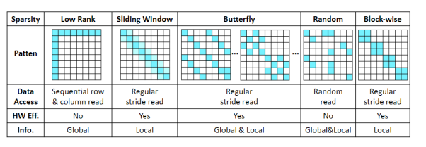
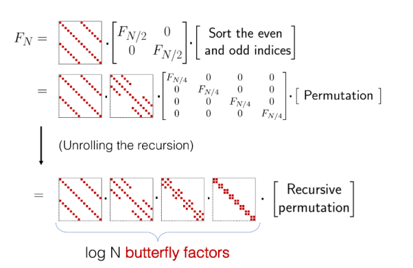
The selection of which matrix compression method to adopt mainly considers several factors. First, whether it is possible to capture both local and global information under a single sparse mode. Second, whether the sparse or compressed model is friendly enough for hardware design. Finally, whether the sparse or compressed mode can support both the attention mechanism and the forward propagation network FFN.Comparing several matrix compression and sparsity methods, the butterfly matrix decomposition model can satisfy the following requirements: the matrix can be represented by the product of log (N) sparse butterfly factor matrices, which can reduce the computational and memory complexity from O (N2) to O (N log N).
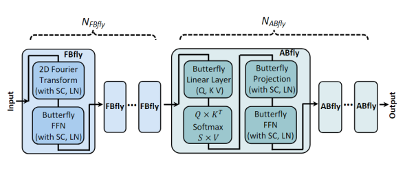
Reference [17] proposed a network architecture called FABNet based on butterfly. The architecture consists of two types of blocks: ABfly and FBfly. The ABfly module mainly achieves this by butterfly transformation, which retains the backbone of the attention module and compresses all linear layers with butterfly decomposition. The ABfly block starts from three butterfly linear layers, generates Q, K, and V matrices, which are then input into a vanilla multi-head attention layer and another butterfly linear layer that obtains the relationships between different tokens, and finally undergoes additional processing by a butterfly feed-forward network (FFN) composed of two butterfly linear layers. In order to further improve hardware efficiency, in addition to ABfly, there is also an FBfly module in the network. In the FBfly module, 2D Fourier transform is implemented through fast Fourier transforms (FFT), effectively mitigating different input tokens, allowing the subsequent butterfly feed-forward network (FFN) in FBfly module to process longer sequences. Although Fourier transforms may cause accuracy loss, it consumes less computation and storage than butterfly transforms. The numbers of FBfly and ABfly in the network can be configured as hyperparameters to seek the best balance between accuracy and efficiency.
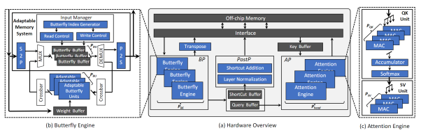
 The adaptive butterfly-shaped hardware accelerator architecture for transformer-based is shown below, consisting mainly of the Butterfly Processor (BP), Attention Processor (AP), Post-Processing Processor (PostP), and on-chip buffer, etc. BP contains multiple Butterfly Engines (BE), which are mainly used to accelerate butterfly transform and fast Fourier transform. AP contains multiple Attention Engines (AE), and each AE is composed of a QK unit and an SV unit. The QK unit is used to calculate the matrix multiplication and softmax between query and key, while the SV unit receives the output from the QK unit and multiplies it with the Value vector to produce the final result of attention.
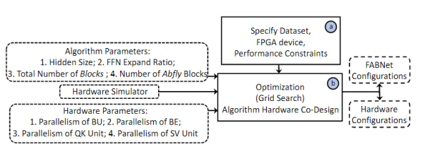
As mentioned above, the number of ABfly modules and FBfly modules in the FABfly network can be configured as hyperparameters. Based on these two parameters, a software-hardware co-design method has been developed as shown in the figure below, realizing the exploration of the design space for neural architecture and hardware design.
Conclusion
This article analyzes the comparison between FPGA, GPU, and ASIC, and concludes that FPGA will not “beat” GPU and ASIC in all indicators to achieve NN. By outlining various solutions for implementing neural network accelerators on FPGA, as well as analyzing two specific instances related to CNN-based and transformer-based, FPGA has unique advantages in software-hardware co-design for model quantization and sparsification. Even though the final product may adopt the form of ASIC for commercialization, FPGA remains the best platform for ASIC digital logic prototyping and testing, as well as technology demonstration.Reference
[1] Y. Zhao et al., ‘Automatic Generation of Multi-precision Multi-arithmetic CNN Accelerators for FPGAs’, 2019, doi: 10.48550/ARXIV.1910.10075.
[2] ‘Real Performance of FPGAs Tops GPUs in the Race to Accelerate AI’, Intel. https://www.intel.com/content/www/us/en/products/docs/programmable/fpga-performance-tops-gpus-white-paper.html (accessed Nov. 13, 2022).
[3] M. Lebedev and P. Belecky, ‘A Survey of Open-source Tools for FPGA-based Inference of Artificial Neural Networks’, in 2021 Ivannikov Memorial Workshop (IVMEM), Nizhny Novgorod, Russian Federation, Sep. 2021, pp. 50-56. doi: 10.1109/IVMEM53963.2021.00015.
[4] Y. Ma, N. Suda, Y. Cao, S. Vrudhula, and J. Seo, ‘ALAMO: FPGA acceleration of deep learning algorithms with a modularized RTL compiler’, Integration, vol. 62, pp. 14-23, Jun. 2018, doi: 10.1016/j.vlsi.2017.12.009.- [5] J. Shen, Y. Huang, Z. Wang, Y. Qiao, M. Wen, and C. Zhang, ‘Towards a Uniform Template-based Architecture for Accelerating 2D and 3D CNNs on FPGA’, in Proceedings of the 2018 ACM/SIGDA International Symposium on Field-Programmable Gate Arrays, Monterey CALIFORNIA USA, Feb. 2018, pp. 97–106. doi: 10.1145/3174243.3174257.
-
[6] K. Guo, S. Zeng, J. Yu, Y. Wang, and H. Yang, ‘[DL] A Survey of FPGA-based Neural Network Inference Accelerators’, ACM Trans. Reconfigurable Technol. Syst., vol. 12, no. 1, pp. 1–26, Mar. 2019, doi: 10.1145/3289185.
-
[7] H. Mujtaba, ‘NVIDIA GeForce RTX 3090, GeForce RTX 3080, GeForce RTX 3070 Graphics Cards Custom Model Roundup’, Wccftech, Sep. 01, 2020. https://wccftech.com/nvidia-geforce-rtx-3090-geforce-rtx-3080-geforce-rtx-3070-graphics-cards-custom-model-roundup/ (accessed Nov. 19, 2022).- [8] A. Shawahna, S. M. Sait, and A. El-Maleh, ‘FPGA-Based Accelerators of Deep Learning Networks for Learning and Classification: A Review’, IEEE Access, vol. 7, pp. 7823–7859, 2019, doi: 10.1109/ACCESS.2018.2890150.
-
[9] Naveen Suda, Vikas Chandra, Ganesh Dasika, Abinash Mohanty, Yufei Ma, Sarma Vrudhula, Jae-sun Seo, and Yu Cao. Throughput-Optimized OpenCL-based FPGA Accelerator for Large-Scale Convolutional Neural Networks. In Proceedings of the ACM/SIGDA International Symposium on Field-Programmable Gate Arrays – FPGA ’16, pages 16–25, 2016.
-
[10] Chen Zhang, Zhenman Fang, Peipei Zhou, Peichen Pan, and Jason Cong. Caffeine: Caffeine: Towards uniformed representation and acceleration for deep convolutional neural networks. In Proceedings of the International Conference on Computer-Aided Design – ICCAD ’16, pages 1–8, New York, New York, USA, 2016. ACM- [11] Yufei Ma, Yu Cao, Sarma Vrudhula, and Jae-sun Seo. “Optimizing Loop Operation and Dataflow in FPGA Acceleration of Deep Convolutional Neural Networks.” In Proceedings of the ACM/SIGDA International Symposium on Field-Programmable Gate Arrays – FPGA ’17, pages 45–54, 2017.
-
[12] Yufei Ma, Yu Cao, Sarma Vrudhula, and Jae-sun Seo. “An automatic RTL compiler for high-throughput FPGA implementation of diverse deep convolutional neural networks.” In Proceedings of the International Conference on Field Programmable Logic and Applications – FPL ’17, pages 1–8. IEEE, 9 2017.
-
[13] Stylianos I Venieris and Christos Savvas Bouganis. “Latency-Driven Design for FPGA-based Convolutional Neural Networks.” In Proceedings of the International Conference on Field Programmable Logic and Applications – FPL ’17, 2017.- [14] Chen Zhang, Zhenman Fang, Peipei Zhou, Peichen Pan, and Jason Cong. Caffeine: Towards uniformed representation and acceleration for deep convolutional neural networks. In Proceedings of the International Conference on Computer-Aided Design – ICCAD ’16, pages 1–8, New York, New York, USA, 2016. ACM.
-
[15] Jialiang Zhang and Jing Li. Improving the Performance of OpenCL-based FPGA Accelerator for Convolutional Neural Network. In Proceedings of the ACM/SIGDA International Symposium on Field-Programmable Gate Arrays – FPGA ’17, pages 25–34, 2017.
-
[16] R. Zhao, H.-C. Ng, W. Luk, and X. Niu. Towards efficient convolutional neural network for domain-specific applications on FPGA. arXiv preprint, 2018.
-
[17] Yufei Ma, Yu Cao, Sarma Vrudhula, and Jae-sun Seo. An automatic RTL compiler for high-throughput FPGA implementation of diverse deep convolutional neural networks. In Proceedings of the International Conference on Field Programmable Logic and Applications – FPL ’17, pages 1–8. IEEE, 9 2017.- [18] Fan, H., Chau, T., Venieris, S. I., Lee, R., Kouris, A., Luk, W., Lane, N. D., & Abdelfattah, M. S. (2022). Adaptable Butterfly Accelerator for Attention-based NNs via Hardware and Algorithm Co-design. arXiv. https://doi.org/10.48550/arXiv.2209.09570
-
[19] B. Li, S. Pandey, H. Fang, Y. Lyv, J. Li, J. Chen, M. Xie, L. Wan, H. Liu, and C. Ding, “FTRANS: Energy-Efficient Acceleration of Transformers using FPGA,” in ACM/IEEE International Symposium on Low Power Electronics and Design (ISLPED), 2020, pp. 175–180.
-
[20] Li, Z., Sun, M., Lu, A., Ma, H., Yuan, G., Xie, Y., Tang, H., Li, Y., Leeser, M., Wang, Z., Lin, X., & Fang, Z. (2022). Auto-ViT-Acc: An FPGA-Aware Automatic Acceleration Framework for Vision Transformer with Mixed-Scheme Quantization. arXiv. https://doi.org/10.48550/arXiv.2208.05163[21] W. Hu et al., “Vis-top: Visual transformer overlay processor,” arXiv preprint arXiv:2110.10957, 2021.
This article is a translation by ChatGPT of a Chinese report from 42HOW. If you have any questions about it, please email bd@42how.com.