In recent times, the global automotive industry has been adjusting their production capacity due to the shortage of chips, which has affected car manufacturers such as Volkswagen, General Motors, Ford, Subaru, Toyota, Nissan among others. According to Bernstein Research, the shortage of chips for cars would cause a loss of production of around 4.5 million vehicles in 2021, which is around 5% of total production.
Wei Zhejia, the President of TSMC, which is a leader in chip manufacturing, mentioned in a press conference that many of their automotive customers cut their chip orders from TSMC in the second quarter of 2020. Consequently, TSMC shifted their chip production capacity to consumer electronics and high-performance chip customer orders. However, in the second half of the year, there was a recovery in demand from automotive customers. Given the long production cycle of the semiconductor industry, TSMC is still struggling to cope with the rebound in demand from car companies. They stated that if they could expand their chip manufacturing capacity, they would prioritize the production of auto chips.
The tone of their words seems indifferent to the automotive industry, as TSMC’s 2020 sales figures indicate that auto chips only accounted for 3% of their total sales. The larger parts of their sales were in consumer electronics (48%) and high-performance chips (33%). In Q4 2020, TSMC’s automotive chipset sales increased by 27% compared to Q3 but still only accounted for 3%. It is evident from these figures that TSMC cares more about their other customers than the automotive industry.
However, this is not the only reason for this situation. If they deploy new production lines at this point, the initial yield rate of the chips will not be too high during the run-in period, which could lead to an increase in production costs and a decrease in efficiency. Manufacturers will not voluntarily take on less profitable business.
Germany, where the automotive industry is a significant sector, could not sit idly by in this situation. Shortly after this development, German Economy Minister Peter Altmaier wrote to the government of Taiwan requesting the supply of auto chips, specifically mentioning TSMC to deliver this message. TSMC’s attitude towards this has subsequently changed, and they have recently stated, “We will continue to work closely with automotive electronic customers to ensure adequate support for their production capacity needs.”
Close collaboration usually requires “speaking with money,” and TSMC and United Microelectronics Corporation have already inquired about the possibility of price increases with automotive component customers such as NXP Semiconductors and Renesas Electronics. According to Japan’s Nikkei Business Daily on January 25, the reason for the price increases is not only the global shortage of car chips but also the fact that the exchange rate between the New Taiwan dollar and the US dollar has increased by 6% in the past year, and the increase in chip prices could be as high as 15%. It is expected to take effect as early as the second half of February to March.But according to informed sources, automakers have larger purchasing power than consumer electronics customers because the gross profit of a single automotive product is higher. In addition, the newly added chip production capacity is also limited. To ensure their automotive production capacity is not affected, even a 20%-30% increase in prices is acceptable to automakers, not just a 15% increase. Furthermore, even the Orin chip with the highest computing power in the automotive industry uses the 7nm process, and as long as it is not the 5nm process, it is acceptable for TSMC to release some capacity to automotive customers.
A small chip can cause so many “heroes” to be at a loss, so let’s start with the birth of a chip.
From Drawing to Design
Chips, also known as integrated circuits, have some similarities and differences from integrated circuits. First of all, integrated circuits emphasize circuit design and layout, while chips emphasize circuit integration, production, and installation. However, the meaning of chips is broader, such as MEMS gyroscopes in our mobile phones and DNA chips in biomedicine.

But the intersection of integrated circuits and chips is the “circuits on silicon wafers”. In general, the principle of a chip is to integrate a circuit on a very small silicon wafer. By designing circuit layout and applying materials, two states of conductivity and non-conductivity can be achieved and recorded, thus achieving the functions of computation and storage.
Speaking of chip design, it is usually divided into two parts: “front end” and “back end”. The front end is mainly responsible for dividing the chip’s functional modules according to the customer’s requirements for the function and performance of the chip, designing the circuit routing preliminarily, and simulating and verifying to test whether the design is feasible. This is similar to an interior designer’s design and simulated effect drawing when we decorate a house.
As for the back end, it is more detailed based on the front-end work, such as planning and placing macro-unit modules, clock routing, parasitic parameter extraction, checking short circuits and open circuits, and ensuring whether the spacing and width of the connections meet process requirements. In simple terms, the back end needs to produce a reliable “construction drawing” and provide it to the factory to start work.
It is worth mentioning that most chip design companies use ARM’s technology architecture authorization, because ARM’s architecture has fewer instructions, simpler implementation, higher compile efficiency, and lower overall power consumption. To put it bluntly, it is like the role of Arabic numerals, which are comprehensible and universally applicable.Here’s a side topic: NVIDIA is attempting to acquire this company for $54 billion. However, its behavior of being both a player and referee is currently under investigation by multiple anti-monopoly mechanisms in various countries. It is estimated that it may take more than a year or two to reach a conclusion. The reason for this acquisition, in my opinion, is not solely based on technological development. It’s like adding some “Maggi chicken essence” when cooking to make the dish taste better and then thinking about buying the “Maggi chicken essence” company.
In addition to the ARM architecture, we also have another option to choose from, which is to switch to other CPU architectures such as RISC-V. In order to maintain the neutrality of the company, RISC-V has moved permanently to Switzerland from the United States in March 2020. For instance, Alibaba’s Xuantie 910 processor, which is built on this architecture, but it brings a problem that chip design companies will have to start all over again in terms of the chip design technology they have accumulated. As a result, the underlying language has changed, with “123” now becoming “One Two Three.” Therefore, this is a difficult choice for chip design companies.
Furthermore, Electronic Design Automation (EDA) software, which is used to automate the process of designing a chip, is worth mentioning. It greatly improves the efficiency of chip design, covering the conceptual design, analysis, IC production, PCB drawing, and other aspects in chip design, as well as in chip manufacturing and testing. For students with design foundations, it is easier to understand the principles through CAD; EDA is used to create three-dimensional circuit diagrams with simple lines on paper.
For example, NVIDIA’s latest Orin chip contains 17 billion transistors, and continuous simulation and verification are required during the design process. Without efficient EDA software, engineers at NVIDIA may burn out during the enormous project of designing a single Orin chip with 170 billion transistors.
Currently, there are only three major players in the EDA software market, namely, Synopsys, Candence, and Mentor, which together occupy more than 90% of the market share. However, the three companies complement each other in technology, and no one company has a monopoly. Huawei, before it was blocked from using EDA software for technological reasons, had used EDA software from all the three companies, depending on different scenarios.But all three companies are American companies that implemented technological blockades against Huawei during the period of Chuan Jianguo, so EDA software is also part of the “neck card”, which means that Huawei is currently using EDA software that has been authorized or purchased before, but cannot be updated to the latest version.
Returning to the topic, EDA software not only improves the efficiency of chip design, but also plays a very important role in the “mask” in the manufacturing process of chips mentioned below, which also requires the use of EDA software.
This is a grain of sand
After the designer completes the “construction drawing”, our house can enter the decoration phase, and the same is true for chips, even the raw materials are somewhat similar, they are all “sand”. Because the raw material for chips is actually “silicon”, and the main component of sand is “silicon dioxide”, which is made more expensive than gold by technical means. This is why chip manufacturing is considered the highest crystallization of human wisdom.
The first step in chip manufacturing is to purify the sand. The basic principle is to add sand and coke in the proportion of chemical reaction in the electric arc furnace with a temperature of 2000 degrees, and then reduce the silicon dioxide in the sand and separate out carbon dioxide and silicon elements. The chemical formula is SiO2 + 2C + high temperature = Si + 2CO. If less carbon is added, a certain proportion of SiC will be generated, which is silicon carbide, which is not discussed here.
The above process can extract silicon with a purity of more than 98% from sand, but unfortunately, the purity of such silicon is still not high enough to be used directly for chip manufacturing because the impurities are still too many and the purity is not high enough, which means that the value of sand is still not high enough.
Because chip manufacturing requires high-purity silicon, the purity ratio must reach 99.999999999%, which has 11 nines, which means that there can be only a few impurity atoms in a few hundred billion atoms on average. Currently, domestic technology can purify to about three nines, which is called “polycrystalline silicon”. At this time, silicon needs to go abroad to study, and companies such as Sumco and Siltronic need to further purify it to 11 nines. Of course, this “study abroad fee” is not low.

As for the further purification process of industrial silicon, the general method is to mix “industrial silicon” with “chlorine gas” and heat it to obtain “silicon tetrachloride”. The chemical formula is Si + 2Cl2 + high temperature = SiCl4.
As for why “chlorine gas” is needed, it is said by professionals that chlorine compounds are generally easier to be purified, in addition to silicon tetrachloride, there are also technical routes such as silicon tetraiodide and methylsilane.After obtaining “silicon tetrachloride”, the next step is to remove the “chlorine element”. Then, in the next step, hydrogen gas is continuously passed at high temperature, followed by a wave to obtain high-purity silicon. The chemical formula for this process is SiCl4 + 2H2 + high temperature = 4HCl + Si. As for why hydrogen gas is added, it is because the principle of redox reaction is utilized. It is easy to obtain high-purity silicon by utilizing the volatility of hydrogen chloride. By the way, the aqueous solution of hydrogen chloride also has a famous name: hydrochloric acid.
Also, during the high temperature process, “silicon” will become liquid. During this step, when the high-purity silicon is completely cooled and solidified, it becomes a highly purified “single crystal silicon”. Then, we use a cylindrical mold to shape it into a “single crystal silicon rod”, and then polish and grind this cylindrical single crystal silicon rod into a suitable diameter, and then we can start “cutting”, which is a bit like “cutting carrots”.
It should be added that with the development of technology, the diameter of wafers has been increasing. In the early 1970s, the diameter of wafers was less than 50 millimeters. It has now increased to over 300 millimeters. As the diameter of wafers gets larger, the number of chips that can be manufactured is also increasing. A wafer with a diameter of over 300 millimeters can be manufactured into more than 300 microprocessors with over 100 billion transistors.
By the way, this is also what is commonly referred to as the 12-inch wafer platform, because 12 inches is roughly equal to 300 millimeters. Then, the wafer is cut, and the “cutting method” is very important in this process. Each cut must be controlled between 0.5-1.5 millimeters.
However, the cut wafer is not delicate enough. As the diameter of the wafer gets larger and the size of the chip gets smaller, and the number of interconnect layers increases, the wafer surface needs to have extremely high flatness, smoothness and cleanliness to achieve multi-layer wiring on the surface of the wafer. “Chemical mechanical polishing” is currently the most effective technique for polishing the surface of the wafer.
I’d like to add that the “chip shortage” phenomenon caused by the epidemic and macroeconomic factors, in addition to production capacity, also lacks “silicon wafers” similar to sliced carrots, because limited production capacity and huge demand for chips lead to fluctuations in wafer prices every quarter.
At this time, the value of sand begins to enter the “middle class”, but it is not satisfied.
Plastic surgery is importantAfter being subjected to high temperatures of several thousand degrees and purified with chemicals, sand is given a new life and its value is multiplied countless times. However, the sand, now transformed into silicon wafers, does not give up its efforts to raise its value further. In order to do so, the wiring of chip design diagrams needs to be copied onto the surface of the wafer, giving it the ability to think for itself. This process is called “photolithography” and is a bit like embarking on the irreversible path of “plastic surgery.”
The process of “plastic surgery” can be said to be the most technologically challenging part of chip manufacturing. Success is “worth its weight in gold,” while failure means starting over.
Firstly, the general process of “plastic surgery” involves coating the silicon wafer with a thin film, applying photoresist, and then using a combination of a mask and a lens to expose the wafer to light, repeatedly going through several processes to trace the circuit diagram of the chip design on the surface of the wafer.
Since chip manufacturing is a nano-level activity, there is no surgical knife that can accomplish such a task. Therefore, we utilize the principle of optical development to transfer the circuit diagram on the mask to the thin film, usually including steps such as photoresist coating, baking, alignment of light exposure, exposure, and development. In short, the process of “plastic surgery” harnesses the burning effect of ultraviolet light in the light, and to increase the intensity of this burning effect, we need a “lens” to help out. This reference to the principle of igniting a fire with a magnifying glass is particularly easy to understand.
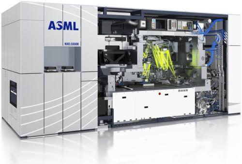
Of course, here we have to mention the famous company ASML, which almost monopolizes all the production capacity of EUV lithography machines.
So how do we get the desired burn effect from the “light”? The “mask” becomes important. Simply put, the mask is the chip diagram mentioned earlier, but it is not for humans to read, it is for “light” to read. The basic principle is to shine a light source onto the convex lens to produce parallel light, and then pass it through a lens underneath to project the light onto the wafer on the worktable. The wafer is coated with photoresist, and after being irradiated by the light, the photoresist is corroded and dissolved, then the surface of the wafer becomes an electrical circuit diagram exactly like the mask, only in a miniaturized version.
At this point, the surface of the wafer has formed uneven “grooves,” and it is now possible to introduce impurities into the wafer’s grooves, namely “boron” and “phosphorus.”The reason for doing this is to ensure that the current can flow during the process. Since silicon itself is not conductive, “boron” and “phosphorus” are needed to help. But interestingly, after adding these two elements, the conductivity of the entire wafer is “unidirectional”, that is, the current can only flow from the region containing “boron impurities” to the region containing “phosphorus impurities”, and the current cannot flow from the region containing “phosphorus impurities” to the region containing “boron impurities”.
We call the above structure a “semiconductor PN junction”. Various gate circuits such as AND gates, OR gates, NOT gates, NAND gates, and NOR gates are added to achieve the output of various processes. The final output is recorded and calculated as “output 0 in power-off and low-voltage state” and “output 1 in conductive high-voltage state”.
This is because the silly machine can only understand the two numbers 0 and 1, which is binary and is also a language for human-machine communication. A hypothesis is that 1101 represents obstacles in front in the language of ADAS. Humans with logical algorithms will cause the vehicle to brake when the chip outputs the 1101 instruction, achieving the braking effect of ADAS.
Returning to the topic, after the “doping” process is completed, the unnecessary substances on the surface of the wafer are removed through dry etching and wet etching techniques. Then repeat the above “plastic surgery” process several times. For example, the 7nm process chip manufacturing requires more than 80 films to be able to etch the structure on the chip design into the wafer. After the design on the drawing is completely reflected on the wafer, metals are deposited on the surface of the wafer by the same method to connect various parts of the transistor. At this point, the “plastic surgery” work is over.
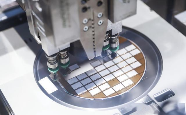
Next is packaging and testing. After the silicon wafer is processed into a chip, it needs to be packaged. Packaging means cutting, cutting the small chip out, putting on a chip protective shell, and then powering on and connecting the signal. Then test the current, heat dissipation, connectivity, and qualification rate of the chip. The technical barriers are not high in this area. Sand has thus completed its journey to the peak of life.### Concluding Remarks
In the entire manufacturing process, chips go through multiple processes, including wet cleaning, photolithography, ion implantation, dry etching, wet etching, plasma rinsing, rapid thermal annealing, annealing, thermal oxidation, chemical and physical vapor deposition, molecular beam epitaxy, electroplating treatment, chemical and mechanical surface treatment, wafer testing and polishing, etc. However, due to length limitations, only a brief summary can be provided. I welcome friends who continue to pay attention to the chip industry to learn and discuss with each other.
Behind the evolution from sand to chips, which has skyrocketed in value, is the continuous development of integrated circuit technology. As electronic devices become smaller and the requirements for performance and power consumption become higher, the manufacturing difficulties of chips also increase.
Currently, the development of the chip industry worldwide is thriving, with star companies in chip design such as Huawei, NVIDIA, Qualcomm, Intel, Broadcom, and MediaTek, and manufacturers such as TSMC, Samsung, UMC, and SMIC. Thus, chip technology is the highest crystallization of human wisdom and civilization, and this phrase is not an exaggeration.
However, in China, chip manufacturing is still our weakness. As Ren Zhengfei said, “Our company can design top-notch chips, but we cannot manufacture them according to our current technical level.”
This is not only due to competition and price pressure from foreign competitors, but also due to the lack of advanced precision manufacturing equipment. Moreover, the most important factor is that the requirements for line width in chip manufacturing processes are at the level of tens of nanometers, with tiny errors in each process. These increasingly high technological barriers also signify that the mission and vision for China’s semiconductor industry to achieve self-sufficiency is a long and arduous journey.
This article is a translation by ChatGPT of a Chinese report from 42HOW. If you have any questions about it, please email bd@42how.com.