
Special Contributor / Zhou Yanwu (Industry Senior Expert)
Editor / Junxinchexin (汽车之心)
Editor’s note: “New Variables” is a column launched by Junxinchexin to share insights from first-line practitioners in the smart car industry. From the perspective of eyewitnesses, it brings you a preview of key variables in the development of smart cars.
On Twitter, \@greentheonly, who claims to be the “green god,” recently released photos of the actual hardware of Tesla’s latest HW4.0.
This information is extremely valuable, as it allows us to get a glimpse of the latest progress and related technological level of the second-generation FSD chip in HW4.0.
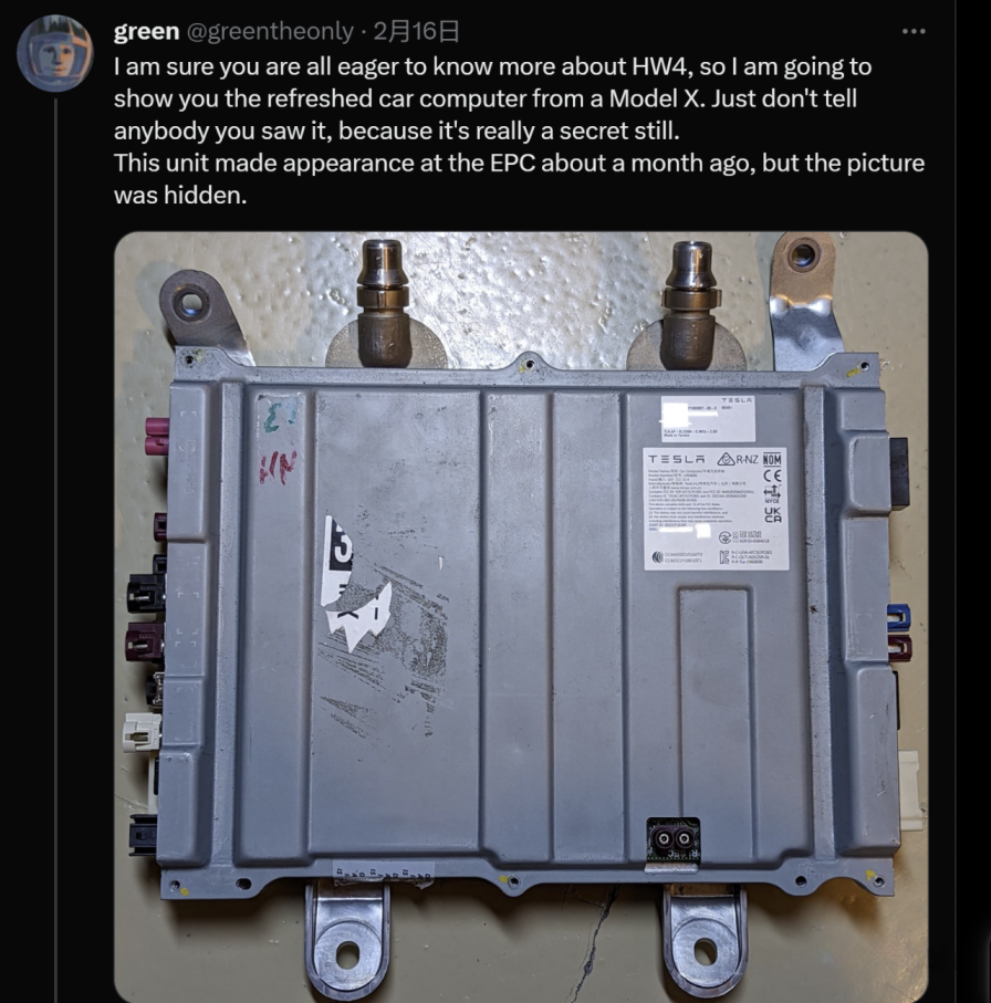
The hardware of HW4.0 was disassembled by the “green god” from the latest Model X model.
It is reported that Tesla’s HW 4.0 will be officially unveiled at the Investor Day held by Tesla and will begin mass production and installation across the entire series.
From the physical hardware perspective, the new HW 4.0 not only has more powerful chips but also has corresponding changes in camera resolution, quantity, and position. In addition, HW 4.0 will also add a 4D millimeter-wave radar.
Tesla’s second-generation FSD is manufactured by Samsung using 7nm process
As early as 2021, there were rumors that the second-generation FSD would be manufactured by Samsung, and there was also a saying that Tesla and Samsung were jointly developing it.
By the second half of 2022, there were rumors again that the second-generation FSD was completed by TSMC, and it was said with certainty that it was 5nm or even 4nm, and there were also rumors that this was the first car-mounted 4nm chip.
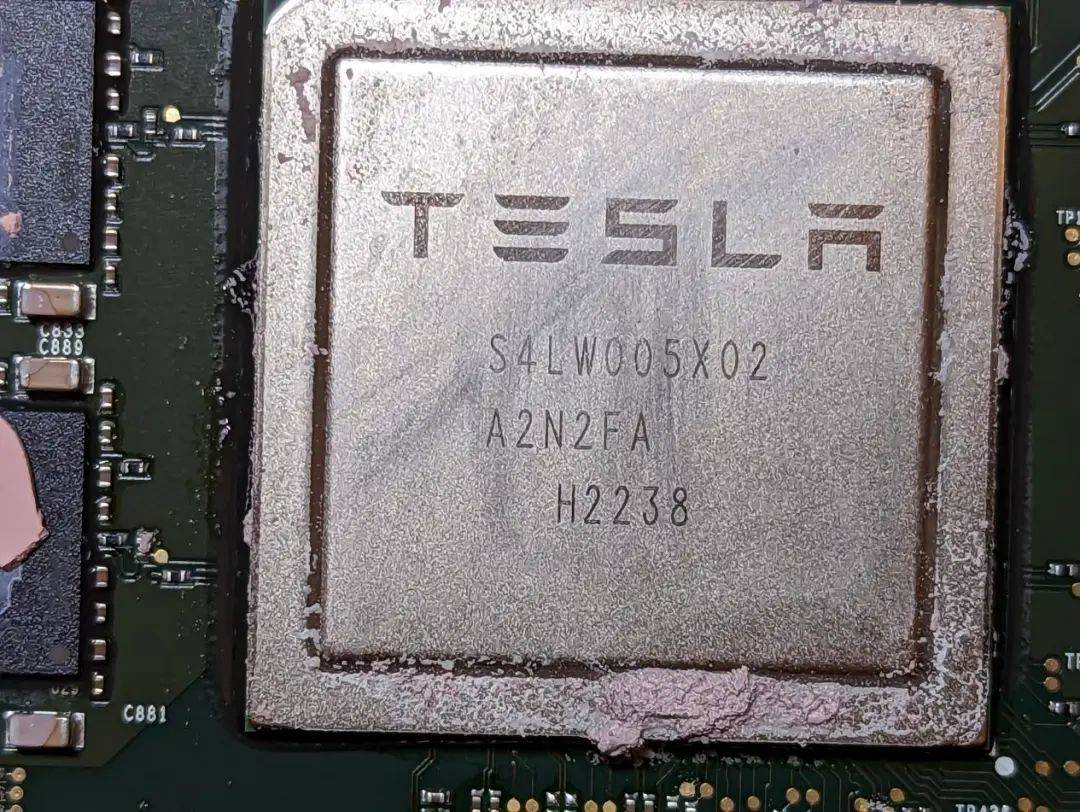
According to the numbers on the surface of the chip, the second-generation FSD chip of Tesla, with the code "H2238", is suspected to be produced by Samsung, and it is very likely to be only 7nm, not 5nm. The information posted on Twitter by Green, "still samsung exynos IP" is incorrect. As we all know, Samsung stopped developing their own CPU architecture in 2015 and currently adopts ARM's public architecture without self-developed IP. The first-generation FSD chip was also manufactured by Samsung, therefore, using the term "still" implies that the second-generation FSD is still manufactured by Samsung. Chip manufacturing and bundling are highly integrated, and if a specific wafer factory is selected for production, both sides need to work together to establish the library for the chip manufacturing process. If the wafer factory is changed midway, the library needs to be rebuilt, which takes a long time and wastes a lot of research and development results.

Why did Tesla choose Samsung? The main reason is probably cost - Samsung's manufacturing price for 7nm chips is less than 1/3 or even 1/4 of TSMC's, and the consequence of Samsung's low-priced grabbing is that the operating profit of the wafer manufacturing department is very low, about 6% in 2021, and around 10% in 2022, while TSMC is almost 50%, which is five times that of Samsung. TSMC's production capacity has always been limited, and compared to Apple, Qualcomm, Nvidia, and AMD's orders that can easily go up to millions or even billions, Tesla's orders are not enough for TSMC. TSMC is also superior to Samsung in 5nm and 3nm manufacturing. Whether in terms of gate or interconnect width, TSMC outperforms Samsung, indicating that Samsung is inferior to TSMC in power consumption.
In addition, there is a geographical advantage as Tesla’s headquarters are currently in Harold Green Road, Austin, Texas, where Tesla’s largest factory and Cybertruck plant are also located. Samsung’s wafer foundry is in the same city of Austin, Texas, which makes communication between the two sides efficient.
In November 2021, Samsung announced that it will invest $17 billion in Texas to build an S2-2 wafer plant in response to the US government’s call. The maximum process node of the S2-1 plant was only 11nm, while the S2-2 plant can achieve 7nm, expected to start production in early 2023. Tesla’s second generation FSD chip is expected to be manufactured by S2-2 foundry.
TSMC is also building a plant in the United States, but the address is in Phoenix, Arizona, and it will not be put into operation until the end of 2024.
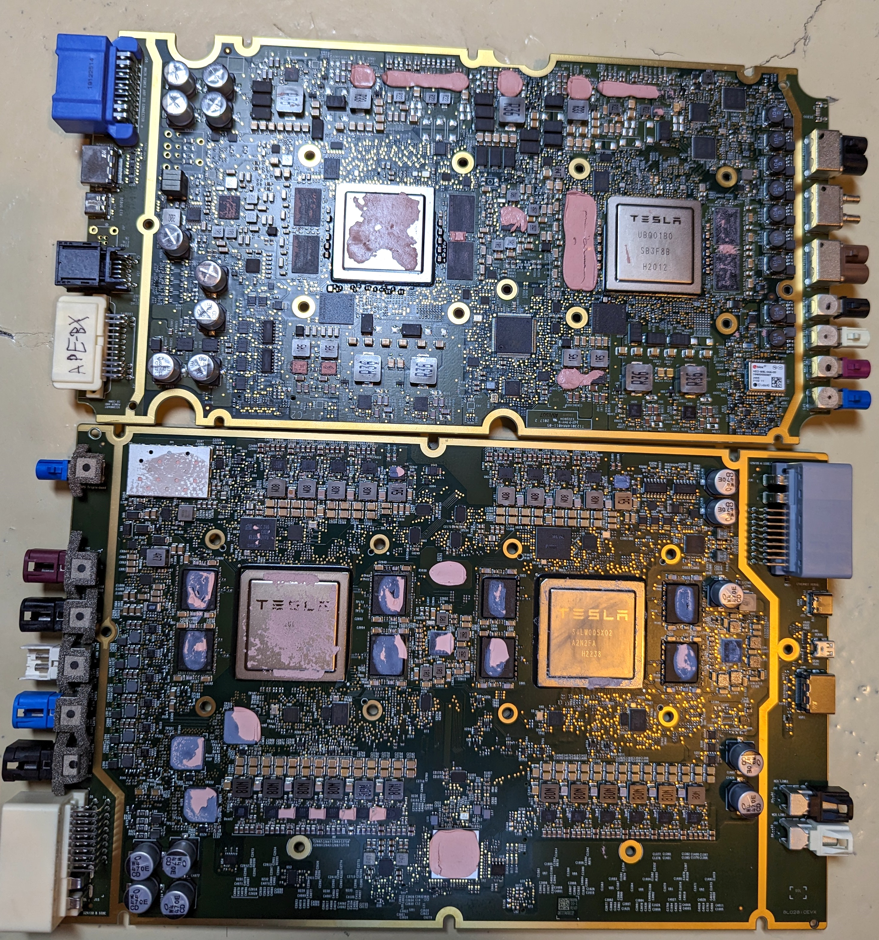
The Tesla HW4.0 frontal PCB shown in the figure above has 20 CPU cores with a running frequency between 1.37GHz and 2.35GHz. In contrast, the first generation FSD had only 12 ARM Cortex-A72 CPU cores. The Cortex-A72 architecture was introduced by ARM in 2015 with performance of around 6.1-6.5DMIPS / MHz, and a maximum operating frequency of about 2.4GHz. Later Cortex-A76, A77, and A78 released by ARM can achieve a maximum operating frequency of more than 3GHz.“`
From the perspective of CPU performance, this also proves that Tesla HW4.0 still uses the 2015 A72.
Calculated according to the initial frequency of 2.2GHz, the computing power of the 20-core A72 is 20*2.2K*6.5=286K, slightly lower than the 12-core A78AE of Nvidia Orin, which is 300K DMIPS.
A significant difference of HW4.0 compared to HW3.0 is that HW4.0 has more components.
HW4.0 has 24 more power supply lines both above and below, especially the 12 power supply lines below. The volume of the inductor is quite large, and the parallel tantalum capacitor array is also impressive (most likely Panasonic’s high-precision tantalum capacitor).
HW3.0 only has 4 power supply lines, while HW4.0 has 20 more lines. I personally speculate that this is because the power of the second-generation FSD has increased significantly. It is estimated that the power of each second-generation FSD is 80-90 watts, or even 100-120 watts. Otherwise, there is no need to increase so many power supply lines.
This also proves that the second-generation FSD uses a 7-nanometer process.
Why is that?
This is actually similar to computer motherboard power design.
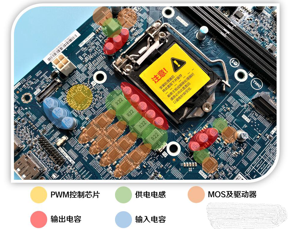
The above figure is a typical computer motherboard. The complete CPU power supply design generally needs to include the above parts.
The PWM chip plays a total control role. Each complete power supply is composed of:
- 1-2 inductors (usually in parallel or multiple phases)
- 1-4 MOSFETs (generally advanced Dr.MOS/2-4 is conventional upper bridge + lower bridge)
“`- Consisting of several filtering capacitors (solid-state capacitors for mid-low-end motherboards, tantalum capacitors for high-end motherboards) and so on.
The power supply of a computer motherboard and a vehicle-mounted computing system is exactly the same: generally a switch circuit.
The switch circuit is a power supply system that controls the time and ratio of switching tube conduction and cut-off to maintain stable output voltage. It mainly consists of capacitors, inductors, MOSFET field-effect tubes, and PWM pulse width modulation ICs.
This circuit system has low heat generation, high conversion efficiency, a large voltage stabilization range, and good voltage stabilization effect.
Generally speaking, a 65-watt computer CPU usually requires 4 or 6-phase power supply, a 250-watt graphics card usually requires 8-phase power supply, and a 500-watt RTX 4070 Ti graphics card usually requires 12+3 (12 GPUs and 3 V-RAMs). Higher-end products require 16+4 phases.
There are many advantages to using multi-phase power supply:
-
It provides greater current;
-
It reduces the temperature of the power supply circuit because the current is split into multiple paths, and the heat generation of each component naturally decreases. The multi-phase power supply circuit can precisely balance the output current of each phase of the power supply circuit to maintain thermal balance for each power component;
-
The core voltage signal obtained by using a multi-phase power supply is more stable than that obtained by using a single-phase power supply.
However, the disadvantage of multi-phase power supply is that the cost is higher, and the requirements for wiring design and heat dissipation are higher. Therefore, the larger the power of the product, the more phases of power supply are required.
Tesla uses 24-phase power supply (estimated 18-phase power supply for two FSDs and 6-phase power supply for V-RAMs). Despite the use of water cooling, the power of the two FSDs is still about 150-200 watts.
And what about Orin? The Orin AGX with 64GB of top-of-the-line configuration has a maximum power of 60 watts.
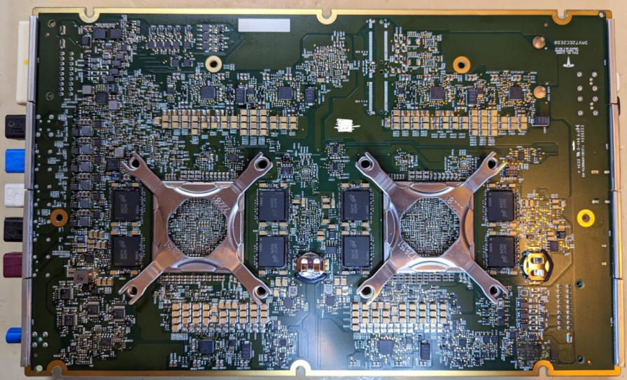
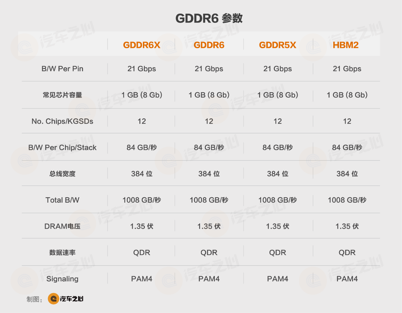
Unlike HW3.0, the backboard of HW4.0 has 8 more memory chips, and FPGA code-named D9ZPR is actually of the MT61M512M32KPA-14 AAT:C model. Tesla spared no expense and used the top-level GDDR6.“`
GDDR, short for Graphics Double Data Rate, is a type of memory specifically designed for graphics cards.
GDDR has its own dedicated operating frequency, clock rate, and voltage, which makes it different from and incompatible with standard DDR memory used in main memory.
Generally speaking, GDDR has a higher clock rate and generates less heat compared to the regular DDR memory used in main memory, making it more suitable for high-end graphics chips.
GDDR is a high-end memory familiar to computer enthusiasts, and GDDR6 was introduced by NVIDIA in their 20-series graphics cards in 2018.
Currently, the most powerful consumer-grade memory is GDDR6X, jointly launched by NVIDIA and Micron in 2020.
However, there is still a significant gap between GDDR6X and HBM2 memory, which is widely used in AI training chips, and of course, HBM2 is much more expensive than GDDR6X.
In the automotive field, LPDDR is currently used, but Tesla has pioneered the use of GDDRR in automotive applications.
Why haven’t other car manufacturers used it before?
One reason is that the computing power demand is not high; second, GDDR has a high power consumption, making it unsuitable for automotive applications.
But Tesla doesn’t care. They put desktop GPUs in cars, so it’s no surprise that they are using GDDR, which has slightly higher power consumption.
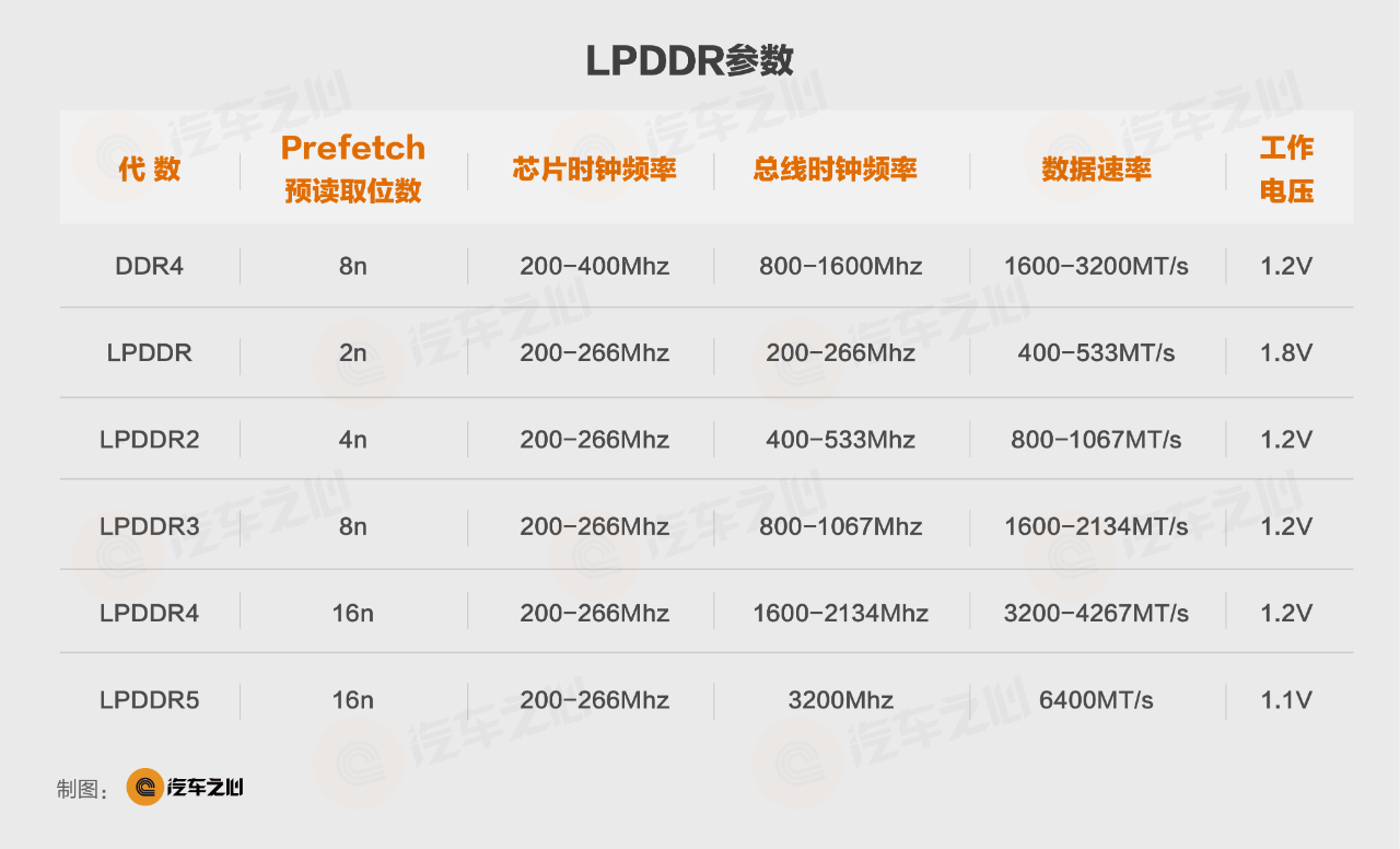
The highest operating frequency of GDDR6 is much higher than that of LPDDR5, reaching up to 1750MHz, with a transfer rate of approximately 12800MT/s, which is double that of LPDDR5, at the cost of double the power consumption of LPDDR5.
Tesla spared no expense, using 16 GDDR6 for a total of 32GB, which is about $200-250 in costs alone. HW3.0, on the other hand, has 8 LPDDR4 chips for a total capacity of 16GB, estimated at about $20.
In terms of flash storage, HW3.0 employs Toshiba's THGAF8G8T23BAIL, a 32GB UFS using older UFS2.1 standard, while HW4.0 opts for Samsung's KLUDG8J1ZD, which offers a 128GB capacity, but still under the UFS2.1 standard.
## How powerful is the second-generation FSD?
For Tesla's "One Shot" type of NPU, increasing computing power is equivalent to adding transistors. To achieve higher density on the same size of the Die, the A72 cores have been increased to 20, which will consume a portion of the Die area. It is estimated that the computing power can be increased up to three times, reaching up to 216TOPS, which is still lower than the Orin.
However, FSD's SRAM capacity is impressive, which is Tesla's consistent feature. The actual computing power of the second-generation FSD is expected to be close to the ideal value.
From the interface alone, HW4.0 at least has two Ethernet interfaces. Judging from the connectors, this is standard single-pair car Ethernet, not the earlier version of Ethernet Audio Video Bridging (EAVB) Ethernet.
Underneath the two FSD chips, there appears to be two car Ethernet PHY chips, likely 88Q2112.
The addition of Ethernet interfaces is specifically for Tesla's 4D millimeter-wave radar, which requires hundreds of megabits of Ethernet to communicate due to the large amount of data produced. Traditional millimeter-wave radar uses CAN or CAN-FD instead.
“`
The Ethernet switch in the middle of the board at the bottom may be Marvell’s 88Q6321.
HW4.0 obviously will not use such relatively outdated and non-strict automotive Ethernet chips.
It is speculated that HW4.0 should be replaced with the more advanced Broadcom BCM8956X or BCM8947X, or it could be from Taiwan, China Ruiyu, because the Ethernet switch on the car board is exactly Ruiyu’s product.
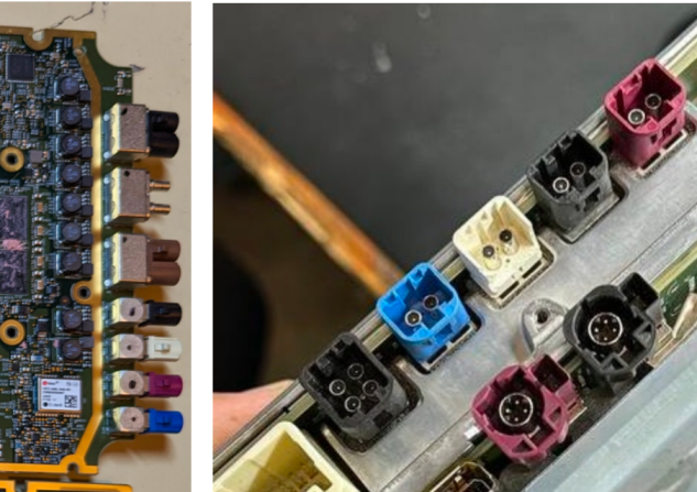
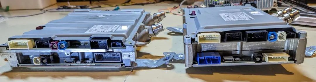
The left picture is the intelligent driving interface of HW3.0. The right picture is HW4.0, the upper layer is the intelligent driving interface of HW4.0, and there are two display output interfaces in the cabin.
Intelligent driving aspect:
-
Red represents the reserved interface;
-
Blue represents driver behavior monitoring.
-
White is for connecting two rear cameras;
-
Black is the front camera, both of which may be 5 million pixels.
In my personal opinion, Tesla HW4.0 reduces one front camera and adds one rear camera.
Tesla used two 4-way deserializers, estimated to be MAX96712 from Maxim, which is very popular in China. There is also one piece that may be 2-way deserializer.
HW3.0 is two chips from Texas Instruments, DS90UB960 and one DS90UB954, which are obviously smaller than MAX96712.
Other differences are not significant, and Spansion’s 64MB Nor Flash is still used as the boot loader.
The power management still appears to be MAX20005 from Maxim. The U-BLOX GPS has been replaced with a higher level of three-band GPS.
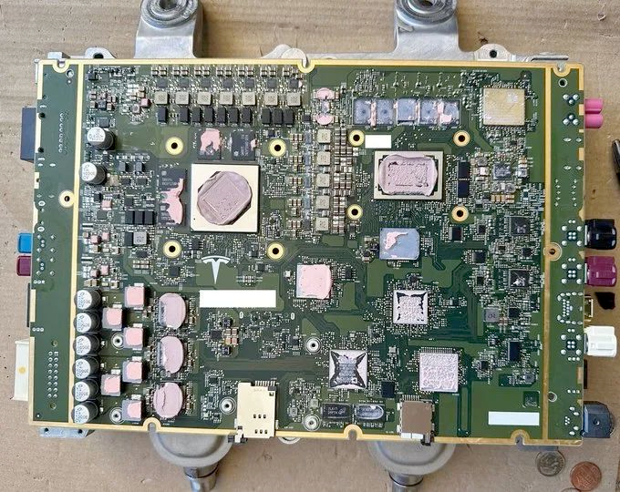
This is the car-machine part of HW4.0, which combines the CPU and GPU into one and puts them on a single PCB board.
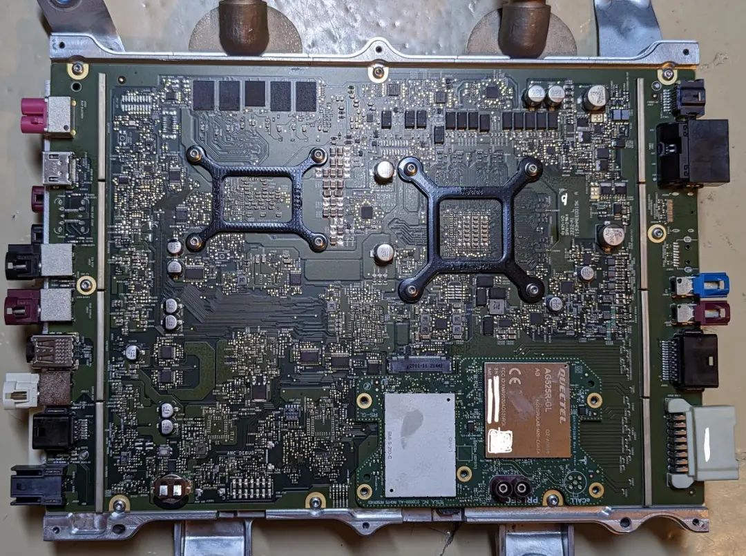
The car-machine backboard for HW4.0 still uses the wireless communication module AG525R-GL, and Bluetooth and WiFi are still LG INNOTEK's ATC5CPC001.
In summary, compared to HW3.0, the following updates have been made to HW4.0:
(1) HW4.0 has a **larger area** and **higher integration** than HW3.0. For example, the car-machine part of HW4.0 combines the CPU and GPU into one and integrates them on a single PCB board.
(2) The core part has not been upgraded much. The CPU core of HW4.0 has increased from 12 to **20**, with a maximum frequency of **2.35GHz** and a default frequency of 1.37Ghz. The number of TRIP cores has increased from 2 to **3**, with a maximum frequency of **2.2GHz**.
(3) The packaging area of the HW4.0 NPU chip has increased, and the power supply has been strengthened. The power consumption of HW4.0 is approximately **twice that of HW 3.0**.
(4) HW4.0 is the first to use GDDR in the car field. HW4.0 upgrades the graphics memory to 16G GDDR6 per core, which exceeds the 8G LPDDR4 per core of HW3.0. It is estimated that the overall computing power of FSD will be **increased by 3-5 times**.
(5) On the PCB board of the domain control module, the number of camera interfaces has increased from 9 in HW3.0 to 12. Specifically, the front-facing triple cameras have been changed to **dual InSight cameras**, which are laid out as follows: 2 side view cameras, 1 front camera, 1 reversing camera, 4 lateral ADAS cameras, and 1 cabin camera, totaling 11, plus 1 spare camera. The forward-facing perception camera has been increased from 1.2 million pixels to 5 million pixels.```
(6) Upgraded GPS module with **three-frequency GPS antenna module** and added L5 frequency to improve positioning accuracy;
(7) Added millimeter wave radar interface and radar heater;
(8) HW4.0 motherboard adopts **symmetrical design** with all configurations in double backup;
Overall, the upgrade of HW4.0 mainly focuses on the FSD chip and sensor architecture.
NVIDIA Orin was launched in December 2019, and Tesla's second-generation FSD is estimated to have started designing in 2020.
In comparison, which one is better, I believe smart readers have the answer.
This article is a translation by ChatGPT of a Chinese report from 42HOW. If you have any questions about it, please email bd@42how.com.