Special contributor/ Zhou Yanwu (senior industry expert)
Editor’s note: “New Variables” is a column launched by AutoHome to share insights from frontline practitioners in the field of intelligent vehicles. From the perspective of insiders, it brings you the key variables in the development of intelligent vehicles.
Tesla’s latest autonomous driving brain FSD spared no expense to use GDDR6.
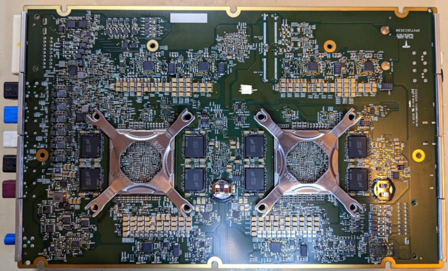
As shown in the above figure, D9ZPR uses 8 chips on each side, totaling 16 chips, with a capacity of 2GB per chip.
But recently, ChatGPT has driven a surge in demand for GDDR6, and prices have slightly increased, currently priced at about 10-13 US dollars per chip.
In fact, the cockpit controller of Tesla HW4.0 also has four GDDR6 chips, each with a capacity of 2GB, for a total of 40GB or more than 200 US dollars.
Most manufacturers choose LPDDR4 or LPDDR5.
For example, Nvidia’s mid-range Orin development box is equipped with four 8GB LPDDR5 chips, totaling 32GB, and only costs about 50-60 US dollars. This is a difference of 150 US dollars from the price of the second-generation FSD in Tesla HW 4.0.
Tesla HW3.0 uses 8 pieces of 2GB LPDDR4 chips, which cost about 3.5 US dollars per chip, with a total cost of only 28 US dollars.
Of course, the biggest winner in this field is Micron, which accounts for 80% of the DRAM market in the automotive industry. Micron is the only memory company in the United States and almost the only hard technology company in the United States, except for Intel (AMD’s manufacturing is done by TSMC).
Overall, LPDDR is currently used in the automotive industry, and Tesla has once again pioneered in the automotive industry by using GDDR for the first time.## What is Memory?
Before discussing GDDR, let’s first understand the concept of memory.
There are two types of storage in computing systems:
One is non-volatile memory (NVM) that does not lose its content even after power-off, and the most common NVM is Flash memory.
The other type is volatile memory that loses its content after power-off, i.e. RAM.
RAM can be divided into two categories:
- DRAM (Dynamic Random Access Memory);
- SRAM (Static Random Access Memory).
Memory typically refers to RAM, which should be more accurately called cache or temporary storage.
Due to the principle of NVM, which is similar to the capacitor, the read and write speeds are very slow, far inferior to the CPU speed. In order to make NVM and CPU work together, memory is added as an intermediate buffer, which can be called the bridge between the RAM calculation unit and the data or instruction storage.
For AI accelerators, memory is particularly important.
The so-called AI operation is matrix multiplication and accumulation, i.e. the product accumulation between the input matrix and the weight matrix, which requires the weight matrix or trained model parameters to be read frequently.
The larger the model parameters, the higher the bandwidth needed, and more parameters can be read out at once.
The robustness and portability of small models are poor, so the development direction of human AI is towards larger and more complex models with more parameters.
The ResNet50, the pioneer of computer vision, has 25 million parameters. The popular Transformer model in the field of autonomous driving ranges from 90 million to 340 million, the ViT variant is 2 billion, and the astonishing GPT3 is 175 billion.
Autonomous driving will eventually reach this scale.
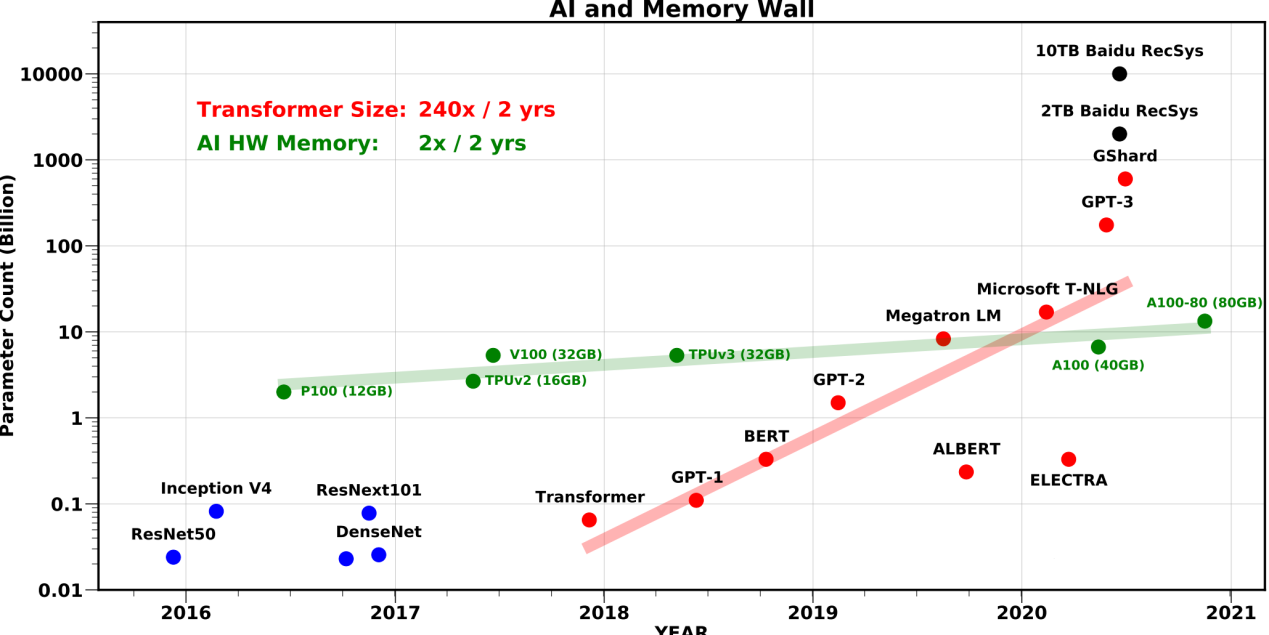 The model will increase by 240 times every two years on average, while memory bandwidth will only double in two years.
SRAM has high speed, and high-performance AI chips require as much SRAM as possible.
SRAM is also expensive, costing around $80-100 per MB. Usually, AI training chips require over 50MB of SRAM, which means a cost of $5000.
SRAM requires 6 transistors and shrinking SRAM is difficult due to the effective width Weff of the channels between the transistors under the current FinFET process.
TSMC’s N3 process, which shrinks about ~5\% compared to N5 (5nm process) with a SRAM bit cell size of 0.0199μm², corresponding to the SRAM bit cell size of 0.021μm² in N5.
The improved N3E (3nm extension) is worse off.
This is because it comes equipped with a 0.021 μm² SRAM bit cell size (roughly translated as 31.8 Mib/mm²), which means there is no scaling compared to N5. Any further extension will increase the cost of the chip without improving performance.
Currently, AI model size is getting bigger and bigger, exceeding 20GB has become commonplace.
Using SRAM for storage, the price of a chip can easily exceed $1 million, which even servers that are not too concerned about price cannot afford.
Therefore, we can only compromise by using HBM, or High Bandwidth Memory, with a cost of approximately $20 per GB.
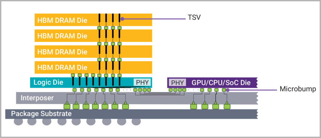
As shown in the figure above, in summary:
HBM stacks SDRAM with TSV (Through Silicon Via) technology, similar to building a multi-storey building, with metal layers and other intervals between layers, all interconnected by TSV.“`markdown
TSV is the key to memory stacking. It can build silicon through holes between storage layers and within layers, and the access of storage unit is completed through these through holes.
Before understanding HBM, we need to understand several basic concepts of memory – density, speed, and bandwidth.
Density refers to capacity.
There are two ways to describe speed: one is frequency, that is, MHz, and the other is MT/s, which is becoming more and more mainstream.
Speed can be thought of as the maximum speed limit on a highway, and bandwidth can be thought of as the number of lanes on a highway.
HBM sacrifices speed to improve bandwidth.
1MHz = 1000KHz = 1000000Hz, which means that the signal switches high and low levels 1 million times in one second.
MT/s stands for Million Transfers Per Second, which means that there are one million transfers per second.
1T/s and 1Hz. The former means that one transfer is made per second, while the latter means one clock cycle per second.
Because the DDR memory signal can be transmitted twice per clock signal, the actual transmission rate is that 1Hz equals 2T/s, and 1MHz is equal to 2MT/s.
After the release of DDR5, the unit for measuring memory performance specifications chose MT/s as the main unit, and leading companies in the PC industry such as Intel, Kingston, Micron, Adata, and G.Skill also adopted this strategy, changing the unit for measuring memory performance to MT/s.
For the CPU, the main data flow is serial, so speed is more important.
While for AI and GPU, bandwidth is more important than speed.
-
Maximum system memory bandwidth = memory nominal frequency * memory bus width * number of channels
-
Actual memory bandwidth = memory nominal frequency * memory bus width * actual number of channels
-
Actual memory bandwidth = memory core frequency * memory bus width * actual number of channels * multiple factor
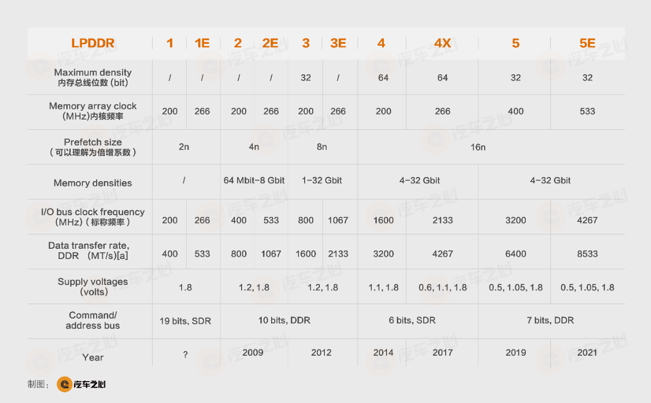
We use LPDDR in the automotive field as an example to describe its bandwidth:
---
Historical LPDDR parameters, note that the bit width is equivalent to the maximum density, which is the maximum data density that the CPU can take away at one time. The maximum density for GPU can easily reach 384bit.
The LPDDR4 used in Tesla's first-generation FSD is model MT53D512M32D2DS-046 AAT, with a capacity of 16Gb and a total of 8 chips. The I/O frequency is 2133MHz. With a single channel, the bandwidth is 2133*64*16, which is **273GB/s**.
HBM adopts physical stacking, and its bus width can be in parallel form. Each Die has 2 channels with a 128-bit bit width. HBM1 has only 4 layers of stacking, called 4-Hi, and the bandwidth can reach 4*2*128=1024bit. The I/O frequency of HBM2 is 1107MHz, and the multiplier is 2.
Taking the NVIDIA V100S accelerator as an example, it uses 4 pieces of HBM2, and the bandwidth is 1107*2*4*1028/8/1000, which is 1134GB/s - much higher than LPDDR4.
When the frequency of HBM3 is raised to 1600MHz, the stacking is increased to 16 layers, which is **four times higher than HBM1**.
The top version of NVIDIA's latest flagship H100 uses 5 pieces of HBM3 memory, each with a capacity of 16GB. The bandwidth is 5*1600*2*16*1028, which is **3350GB/s**.
HBM is connected to the main processor through the silicon interconnection layer of the substrate, which is much closer in physical distance than the memory-to-processor connection on the PCB, almost approaching the connection distance of L3 cache. Although its operating frequency is not high, its speed is a real speed with no water added.
```
Additionally it should be pointed out that DDR includes memory storage technologies such as LPDDR and HBM, with its true core frequency being quite low, between 133MHz and 200MHz.
Yet for the sake of aesthetics, there are barely any manufacturers that mention its core frequency.
An increase in core frequency leads to a significant increase in power consumption, which is the true reason why memory speed has remained relatively slow.
_20230303013219.png)
Here is a high-definition image of H100:
The H100 is divided into two types: **SXM** and **PCIe**.
H100 SXM5 peak INT8 computing power can reach 4000TOPS, while PCIe is 3200TOPS.
Take note of the six tightly attached chips next to the main chip of H100 (one is empty, for symmetrical heat dissipation design, actually only 5), those are the expensive HBM3 chips, provided by SK Hynix of Korea.
Currently, only SK Hynix can mass produce HBM3 and only NVIDIA is a customer.
The downsides of HBM are its expense, its 3D stacking requirement, and poor heat dissipation.
Due to its stacking, and given the relatively high cost, only the server and AI training fields use HBM, not yet the inference field.
One step down from HBM is today's star of the show: **GDDR**.
## Why did Tesla spare no expense using GDDR6?
GDDR can be described as the cheap version of HBM.
GDDR stands for Graphics Double Data Rate and is memory designed for GPUs.
GPUs and AI processors don't have the concept of L1/L2/L3 level cache because they have too many cores, they can't afford to assign cache to every core, since that would be too expensive.
GDDR matured completely by its fifth generation. The previous four generations were based on the traditional DDR and were short-lived flashes in the pan, while the lifecycle of GDDR5 has already exceeded **10 years**.```
GDDR5 improves the maximum frequency by quadrupling, using the so-called QDR technology. DDR is **half-duplex**, while QDR is **full-duplex** with two data buses, both of which can be read and written simultaneously.
For example, GDDR5 usually has an I/O frequency of 1750 MHz, and the actual I/O frequency is 1750\*4=**7000MHz**. The bandwidth of a single GDDR5 is 32\*7G/8=**28GB/s**.
GDDR6 goes further by increasing the prefetch size from 8n to 16n, doubling the bandwidth, and a single bank typically can achieve 56GB/s.
Taking Tesla's 16 GDDR6 chips as an example, the bandwidth is 56\*16=896GB/s, more than three times the bandwidth of the first generation LPDDR4, but still very different from HBM3.
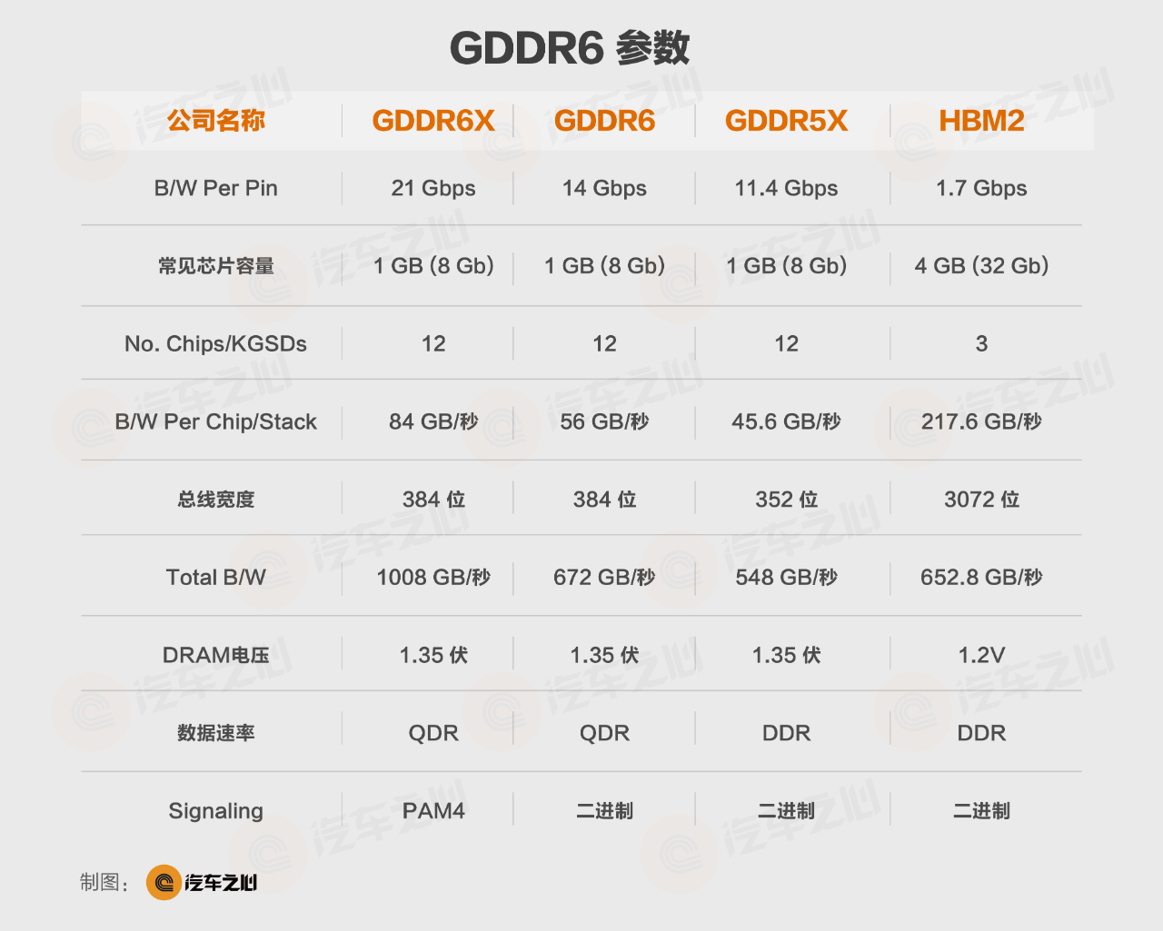
The above figure shows the comparison of various GDDR parameters:
GDDR5X has a bus width of **352 bits**, which supports up to 11 parallel GDDR chips with 32 bits at the maximum, with a total bus width of **352 bits**.
GDDR6 supports up to 12 parallel GDDR6 chips with 32 bits at the maximum, with a total bus width of 384 bits.
GPUs perform parallel computing, which is more difficult for CPUs to achieve with such a high bus width.
GDDR6X appeared in 2019, which is a preview version of GDDR7. The biggest change is the introduction of PAM4 encoding, and a single GDDR6X chip can achieve 84GB/s, while the bandwidth of 12 chips exceeds **1TB/s**.
Although theoretically, GDDR6X adopts PAM4 signal modulation and MTA encoding technology, which significantly improves the energy efficiency.
Same 8 memory chips, GDDR6X has a 15% lower energy consumption per bit compared to GDDR6.
In actual testing, the memory power consumption of RTX3080 with 10GB GDDR6X reaches as high as 70W, and that of RTX3090 with 24GB GDDR6X even goes up to 130W, which is a true power consumer.
However, both GDDR and HBM are designed for parallel computing, focusing on bandwidth rather than speed.
GDDR6’s CSA latency is more than 2 times that of DDR4, which means that GDDR and HBM are not suitable for use on CPUs.
CPU is mainly characterized by sequential computations, therefore the CPU part of NVIDIA’s Grace Hopper Superchip still uses LPDDR5X.
The device with the highest computing power in the world is the NVIDIA DGX-H100, priced at about $250,000. The CPU part uses Intel’s Sapphire Rapids, i.e. Xeon W3XXX series (the flagship product costs nearly $6,000 per piece).
The previous DGX-A100 used AMD’s EPYC Rome as its CPU.
Corresponding to the CPU is SK Hynix’s DDR5. Of course, Intel’s Xeon can also perform parallel computing since it has 56 cores. Therefore, Intel’s Sapphire Rapids also supports HBM2E, but DDR5 is still the preferred option.
Tesla’s second-generation FSD also has a CPU part, i.e. the 20-core ARM Cortex-A72.
But Tesla pays even more attention to AI computing power, or we can say that Tesla has an anxiety over computing power.
“““
NVIDIA is too powerful in computing power. Even though Tesla sacrifices some CPU, it still uses GDDR6 at any cost.
Tesla is keen on large models. In order to ensure high enough efficiency, I speculate that the third-generation FSD chip of Tesla will likely use expensive HBM3, and at least full-weight models need to be installed, with estimated capacity of no less than 50GB.
The cost of this part alone is no less than $1,000. The minimum cost of Tesla’s third-generation FSD in the future is also more than $1,500.
Similarly, if the autonomous driving industry is still keen on artificial intelligence, the cost of the autonomous driving chip in 5 years will be at least $2,000 or more.
“`
This article is a translation by ChatGPT of a Chinese report from 42HOW. If you have any questions about it, please email bd@42how.com.
