
Writing by | Zheng Wen
Editing by | Zhou Changxian
TSMC investing $40 billion to build a factory in the US is a big deal in the chip industry.
At the opening ceremony a few days ago, TSMC’s founder, 91-year-old Zhang Zhongmou, gave a speech. In his speech, he said:
“The ceremony is called the First Tool-in Ceremony. Outside of Taiwan, no one knows what this means, so it was renamed the opening ceremony. This is a common ceremony in Taiwan. At first, I didn’t know what this ceremony represented, but after experiencing many Tool-in ceremonies, I finally understood the meaning of this ceremony.”
“It represents the end of the beginning.”
“For a semiconductor factory, the end of the start-up phase represents the disappearance of the romantic idea of building a factory and the excitement of starting up, leaving many difficult problems to be solved.”
“… Globalization is almost dead, and free trade is almost dead. Many people hope that they can come back, but I think that at least for a period of time, they won’t come back.”
As the world’s largest chip foundry, even a powerful company like TSMC faces numerous challenges and uncertainties in building a new factory in the US.
This event implies two metaphors for us. First, the semiconductor industry is a highly barriered industry, presenting huge challenges for any participating company. Second, TSMC’s establishment of a factory in the US marks the beginning of a deep coupling with the US manufacturing industry, and domestic substitution may be a topic that we must consider and put on the agenda.
Coincidentally, recently, Hei Zhi Ma Intelligence held a technology open day and media communication meeting in Shanghai. “AutocarMax” took this opportunity to gain an in-depth understanding of the development of autonomous driving chip technology.
Today, by tracing “how a domestically produced high-performance intelligence driving chip came into being”, we will together understand and reflect on the difficulties and opportunities in the development of China’s chip industry. How much further do we need to go?
Open the window of opportunity from the car
Firstly, let me provide a brief overview of the IC industry chain, which is composed of three major sections: supporting, core, and demand. The upstream supporting industry chain includes materials, equipment, and clean engineering, which provides necessary tools, raw materials, and production conditions for the production of chip products.
The downstream demand industry chain is the fundamental driving force behind the industry’s development. From mobile phones to PCs, to smartphones, to automotive electronics, 5G, AI, IoT, etc., the industry is constantly advancing in the rolling demands of upgrading and iteration.
The core industry chain, which bridges the upstream and downstream industries, includes the design, manufacturing (front-end wafer processing), and packaging testing (back-end) of semiconductor products.
The prerequisite for the development of an industry is undoubtedly the driving force of market demand. Based on the transformation of new energy and intelligence, the current Chinese automotive industry has a clear market opportunity.
According to statistical data, by 2022, the average number of chips per new energy vehicle will be around 1459, while the number of chips used in traditional fuel vehicles will be 934. Strategy Analytics predicts that the average silicon content per vehicle will double from USD 530 per vehicle in 2021 to over USD 1000 by 2028, more for high-end vehicles, even exceeding USD 3000.
An obvious phenomenon is that the penetration rate and penetration speed of L2 and above-level autonomous driving for new cars in China are leading the world. The Chinese market has a higher acceptance rate for intelligent vehicles, with a more important view of the importance of autonomous driving and a willingness to pay premiums for autonomous driving, which is better than the global average… This provides an excellent soil for the rise of China’s intelligent automotive industry.
Yang Yuxin, the Chief Marketing Officer of Hezhima Intelligence, said that intelligent driving is definitely the most important jewel on the crown of intelligence, and China’s development speed in autonomous driving technology will be far ahead of the world. “By 2025, 66% of new cars in China will be equipped with L2-level or above autonomous driving functions, among which 50% are L2-L3. We believe that human-machine co-piloting will be the norm in the next 3-5 years.”
With the rapid development of intelligence, there has been a significant change in the upgrade cycle of automotive hardware products, which has been shortened from 5-10 years per generation to the current 2-3 years, encouraging more companies to join in.Under the drive of the demand-side industry chain, many companies have seized the opportunity to join the core industry chain, such as Black Sesame Intelligence, Huawei, Horizon, and Xinyu Technology, which are new chip design companies that have entered the race track.
The underlying logic of these companies is that intelligence will revolutionize the automotive industry, and the accumulated mechanical technology of the past is difficult to empower the future. The E/E architecture of the car must be broken and then rebuilt.
In the traditional automotive distributed E/E architecture dominated by “mechanization”, the ECUs are isolated from each other, and the upgrading of vehicle functions depends on the increase in the number of ECUs. After the rapid development of intelligence, the traditional architecture based on the increase in the number of ECUs can no longer meet the needs of functions, computing power, and other requirements.
The E/E architecture has undergone a fundamental change in the evolution of the “electronic” logic, and the isolated status of ECUs must be opened up, and the software and hardware on the car must gradually be decoupled. At the current stage, many E/E architectures will classify intelligent driving as a domain, and classify cabin control as another domain. The whole domain requires a high-performance chip to control it.
In the exploration stage, pioneers used general-purpose processors to handle it, which is to use the “bring-your-own-device” approach and borrow chips from other industries. For example, Google used CPUs to promote AI projects, and Baidu’s DepthLab used GPUs to run deep learning algorithms.
Although GPUs are better than CPUs, they are not easy to use. Since they are essentially general-purpose processors, the shortcomings are obvious in areas where computing demands are more specialized, and the unit computing performance is not as strong as that of purpose-specific processors.
Therefore, the autonomous driving AI dedicated chip was born, and companies such as Black Sesame Intelligence and Horizon joined the race track to achieve their missions.
This chip is like a versatile tool that can handle everything, including image processing, graphics, audio, deep learning, and contains modules such as central processing unit (CPU), graphics processing unit (GPU), image processing unit (ISP), neural processing Unit (NPU), digital signal processor (DSP), etc.
Yang Yuxin believes that only by deeply understanding various IP can a useful chip be designed.Although the difficulty has increased significantly by transitioning from MCUs that emphasize control to versatile SoC chips that emphasize computation, it also means that the requirements for the chips themselves are more complex and higher. Therefore, in the automotive chip industry, areas such as CPU, GPU, ISP, and NPU will all become important directions for innovation.
For example, based on specialized domains, Horizon Robotics has developed two major IPs: NeuralIQ ISP image signal processor and DyanmAI NN engine (NPU) for deep neural network algorithms. The former allows cars to “see more clearly,” while the latter allows cars to have “greater processing power and higher efficiency.”
Another high-performance chip company, Horizon Robotics, has developed its core technology, the high-performance automatic driving processor BPU computing architecture, and optimized its memory architecture. The processor can transmit data freely and perform various calculations, allowing different components to operate simultaneously and improving AI computing efficiency.
Their proprietary technology includes high-performance, low-latency data concurrency processing, pulse array to increase data parallelization speed, and process computing to break through some memory walls to achieve higher technological efficiencies. It is worth mentioning that this architecture has opened its IP authorization this year to meet the chip research and development needs of car companies with strong independent research capabilities.
Horizon Robotics co-founder, Huang Chang, pointed out that “if you are detached from the application scenario, continuous algorithm iteration, and pre-estimated algorithm, then you have no idea of the scale and size of each thing. By focusing on the application and the selection of algorithms, you can more accurately make choices about chip architecture, size, and component mastery.”
This naturally leads to the process of IC design, which includes front-end logical design and back-end physical design.
The front-end includes determining market positioning, determining performance and functional goals, architecture and algorithm design, task division, purchasing IP, RTL coding and functional verification, synthesis gate-level simulation, and static timing analysis and simulation. The back-end involves RTL to gate-level netlist conversion, data import, layout planning, unit layout, clock synthesis tree, wiring, physical verification, and layout file delivery to wafer foundries.If you find the process above difficult to understand, you can use an intuitive example to understand the IC design process.
This process is a bit like building a house. First, you need to determine whether you are building a villa or an affordable housing. Based on this, the overall design scheme of the house is determined, including the area, cost, and location. After these are determined, the parameters such as the floors, number of rooms, and functional layouts of each room need to be further designed… These can be called architecture design.
After the architecture design is completed, the design of each room needs to be further followed up. This part can be called unit design. In the process of room design, it is necessary to check whether it is consistent with the initial design plan, whether the functions are achieved, and whether the specifications of the electrical appliances and furniture are consistent with the preset ones. This part is a process of designing and checking, and the work of checking is called verification.
After each room is completed, the functional modules are basically perfect. The next step is to integrate all the functional modules, connect them together, and test whether the overall functions can work smoothly. After the entire process is completed, a design diagram is formed and handed over to the construction company for construction.
The design of the autonomous driving chip needs to consider how many sensors to connect, what functional processing to do with the data after the connected sensors, and then which IPs are used in the verification, how these IPs are implemented in the architecture design, and finally through the last simulation verification, this is the front-end simulation design.
To implement the design on the chip, it is necessary to consider how to implement the function on the chip, which IPs to use, how to layout the circuit on the chip when the chip is only a few square centimeters. After the chip is produced, testing needs to be done. When designing, it is necessary to consider what tests will be done, so there are many reserved test points on this chip.
After the design work is completed, the next step is to hand it over to TSMC to complete the actual production.
Challenging Moore’s Law
A talk given by Gordon Moore, one of the founders of Intel, became the golden rule of the development of the semiconductor manufacturing industry: The number of transistors that can be accommodated on an integrated circuit will double approximately every 18 to 24 months. That is to say, the performance of processors doubles approximately every two years, while the price drops to half of the previous price.The fast iteration and large investment inevitably lead to significant top-heavy effects in this industry. According to IC Insights’ data, TSMC accounts for more than half of the market share in the top ten contract manufacturers worldwide, and the top eight companies have a market share of nearly 90%.
At the same time, the industry has gradually given rise to the relatively stable Fabless+Foundry+OSAT model. Fabless (design companies) submit the designed circuit diagrams to Foundries (contract manufacturers) for production, and then outsource packaging and testing to OSATs (outsourced assembly and test companies). The final product chip is sold as a Fabless product. Among them, Foundry occupies a dominant position in the industry.
A more intuitive name for chips is integrated circuits. The manufacture of chips is a true “turning lead into gold” process. Let’s go through the process of chip manufacturing first and then discuss the difficulties and characteristics of automotive chips.
Starting with silicon dioxide, the process of wafer manufacturing is not discussed here. Simply put, silicon dioxide is reduced to obtain a silicon ingot, which is purified and then pulled into single crystal silicon rods. They are then sliced and ground into wafers containing colorful 8-12 inch integrated circuits.
Photolithography is a very complex part of the chip manufacturing process. Photolithography etching uses light of a certain wavelength to engrave corresponding marks in the photoresist, thereby changing the chemical properties of the material at the etched site. Each step of the etching process is complicated and elaborate. After many etching steps, the final product is integrated circuits of about 100 square millimeters on the wafer.
The chip manufacturing process has long since entered the nanometer era (nm) from the micron era. This “nm” refers to the size of transistors, and the smaller the transistor, the more units can be placed in the same area.
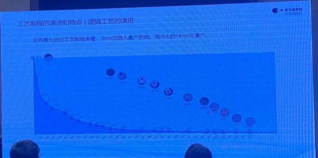
In 2020, TSMC released the ADEP based on 7nm, which is a cutting-edge process automotive platform; in 2022, TSMC released a 5nm automotive process platform.From the perspective of the most advanced production processes in the industry, 3nm has entered the mass production stage. In June of this year, Samsung officially started mass production of 3nm technology. In China, about 14nm can be mass produced, and the industrial process of the supply chain is 28nm.
With the further evolution of Moore’s Law, it is becoming increasingly difficult to carve complex integrated circuits in small areas. For example, with the evolution of CMOS technology, the gate oxide thickness must also be continuously reduced. When the thickness is thin enough, the gate oxide is no longer an ideal insulator and noticeable leakage occurs. Gate oxides are used to achieve electric current paths and are a medium for field control.
Therefore, when 40nm entered 28nm, the industry generally started using HKMG technology, and the technology route was divided into Gate-first and Gate-last. When the process entered 16nm/14nm, the transistor structure changed from 2D to 3D FinFET, which can bring better leakage current control and better performance. Currently, the most advanced mass production process is mainly 7nm/5nm, and smaller pitches make EUV technology increasingly mainstream.
The name GAA (Gate All Around) comes from the structure of the transistor. This new design completely wraps the gate electrode around the channel, which can achieve better control. Samsung will adopt GAA technology earlier than TSMC. TSMC will use GAA starting from 2nm.
After discussing chip manufacturing, let’s talk about the characteristics and difficulties of manufacturing chips for automotive standards, which have higher barriers to entry than other industries. Wang Zhizhong, Director of Black Sesame Intelligent Product Market, introduced that there are many differences between automotive standard chips and consumer chips. One of the difficulties is that the usage environment of cars is much harsher than that of consumer electronics.
It requires the following characteristics: a wide temperature range, with a temperature range of -40°C to 150°C in the engine compartment, -40°C to 125°C in the body control area, and -40°C to 105°C in other body positions, which is much wider than the temperature range of consumer electronics.#### Physics/Chemical Properties Need to be Stable
Stability of physics/chemical properties is required due to the large variation in working environment of vehicles, considering factors such as humidity, dust, salinity, mildew, alternate high/low temperature, vibration, shock, etc.
High Anti-Interference Requirement
The electronic devices, sensors, and various communication harnesses loaded on the vehicle have very high requirements for ESD electrostatic, EFT group pulse, RS conductive radiation, EMC, EMI, etc.

Furthermore, the supply cycle of the automotive grade chips must be guaranteed, and the chips should have 10 years of stable supply, ensuring that there are are no problems with the chips within 15 years.
Long Service Life with High Fault-Tolerance
As for the service life, the requirements should satisfy the design life of 15 years/500,000 km for automobiles, which is much higher than that of consumer electronics such as mobile phones. The fault rate requirement is PPM (parts per million) – PPB (parts per billion)- 0.
High Consistency Requirement
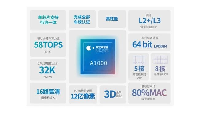
In addition to the above standards, there are also requirements for quality management, reliability, functional safety, environmental protection, etc. For example, the black sesame intelligence A1000 conforms to the ISO-26262 safety standard.
A dedicated server is used to store design documents and process data, and all processes are traceable. On the production line that makes components according to the specific requirements of automobiles, all records must be saved for more than ten years.
High Manufacturing Barriers
Various stringent conditions determine the high barriers to automotive grade chip manufacturing.
According to the analysis of Morgan Stanley’s team, with the continuous evolution of the competition landscape of wafer foundry, the chip competition in the future will mainly take place among TSMC, Samsung, and Intel. The competition in the high-end process market is very fierce. Once behind, instantaneous customer loss can be caused.
The fierce competition of “either you live or I die” drives the continuous progress of semiconductor technology, and brings about the improvement of PPA (performance power area), thereby improving the key indicators and user experience of chips and system products.# PPA, the ultimate KPI for chip developers, has a decisive impact on the high computing power required for intelligent driving chips.
Speaking of which, it can be understood that there is a common saying in the semiconductor industry, “there is no perfect chip, only a perfect balance.” Designing chips largely means finding a balance, balancing process level and chip process, performance and power consumption, computing power and cost…
It’s difficult.
In conclusion:
The mass production of automotive chips is a long and arduous process.
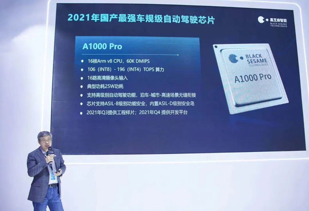
Taking the Huawei Shan’er A1000 series chip from Heizhima Intelligence as an example, from product design, tape-out, certification and algorithm toolchain development to functional safety certification, autonomous driving software package development to perfect support for the industry ecosystem, crossing multiple thresholds, it has experienced more than three years of time.
At the same time, it is also a costly industry that requires sufficient funds for process flowchip fabrication. According to IBS estimates, the total cost of developing a chip, including IP licenses, EDA software, R&D, tape-out, packaging, and testing costs, is USD 106 million for the 16nm technology node, USD 298 million for the 7nm technology node, and USD 542 million for the 5nm technology node.
The future of this industry depends on the participation of deep-digging industry participants who work hard and struggle hard. Currently, it is very critical to lay out and keep up with the pace of advanced semiconductor processes.
Based on the domestic supply chain system including chips, components, software and many other things, Wang Zhizhong introduced, “We are now working on a whole set of national reference designs based on Heizhima chips. To be honest, it will take some time before this thing can truly be implemented in cars. There are different difficulties, including some chips that currently cannot reach the level of automotive-grade …”
Yang Yuxin added, “But we need to find potential partners with cooperative value, and we first form a set of solutions based on self-capability, including operating system, which we have adapted. Everyone gradually makes the system more perfect together, which is a relatively long-term process.””We are pleased to see that many domestic chip companies have already reached key positions, it just takes time to mature or when true mass production will be achieved. We are willing to share our know-how and cooperate with partners for development.
According to Yang Yuxin’s judgement, for companies hoping to replace imports with domestic production in the chip industry, the key time node is 2025. If successful substitution cannot be achieved before 2025, it will be very difficult afterwards.
“For car manufacturers, there are already domestic suppliers for mass production. Their willingness to replace it with another domestically-made product will significantly decrease. Therefore, I think that 2025 is a crucial time node.”
This article is a translation by ChatGPT of a Chinese report from 42HOW. If you have any questions about it, please email bd@42how.com.