This morning, NVIDIA announced the release of the brand new Hopper architecture to replace the Ampere architecture launched two years ago at the 2022 GTC conference. At the same time, NVIDIA released its first GPU based on the Hopper architecture – NVIDIA H100, and a new generation of acceleration computing platforms.
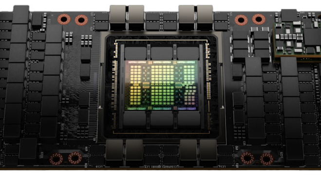
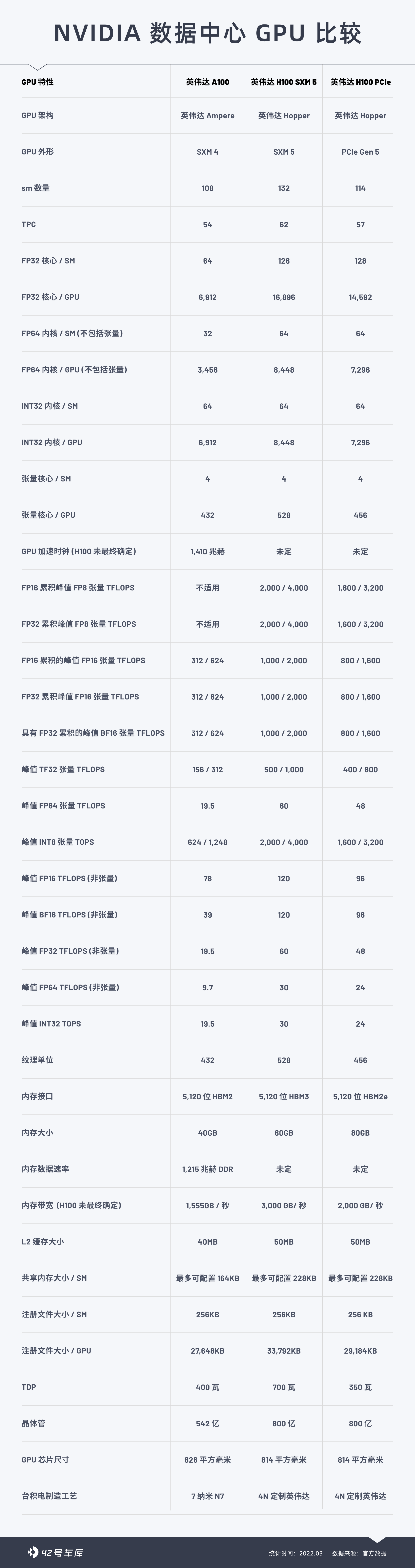
H100 is NVIDIA’s 9th generation data center GPU, adopting the brand new Hopper architecture that is customized by TSMC with NVIDIA 4N technology. It has 80 billion transistors, 8 groups of graphics processing cluster, 72 groups of texture processing cluster, 144 groups of Streaming Multiprocessor (SM), and each group of SM contains 128 FP32 CUDA cores, totaling 18,432 cores.
H100 inherits the design logic of A100 and improves the expandability of AI and HPC workloads. It supports PCIe 5.0, the fourth-generation NVLink, and the bandwidth of the latter is increased to 900 GB/s with a total external bandwidth of 4.9 TB/s. The performance of H100 with InfiniBand interconnection technology is 30 times higher than that of the previous generation A100. According to NVIDIA’s promotion, 20 H100 GPUs are enough to support the global network traffic.
At the same time, the brand new NVLink Switch System interconnection optimized the computing efficiency across multiple GPUs, and in some cases, the performance of H100 using InfiniBand is again increased by three times.
NVIDIA H100 GPU Key Features Summary
-
The performance and efficiency of the brand new Streaming Multiprocessor (SM) are improved, with higher acceleration frequency and more SM numbers. Compared with the previous generation, the new generation Tensor Core is twice as fast as the A100 Stream Processor on the equivalent data type of MMA (Matrix Multiply Accumulate) calculation rate, and FP8 floating-point performance is four times that of A100.
-
The speed of dynamic programming algorithms is up to 7 times faster than that of A100 GPUs.
-
The processing speed under FP64 and FP32 formats is triple that of A100, and the processing efficiency is improved by 2 times.
-
The new thread cluster function allows local programming control.
-
The HBM3 memory subsystem has twice the bandwidth compared with the previous generation. The H100 SXM5 GPU is the world’s first GPU equipped with HBM3 memory, capable of providing 3 TB/s memory bandwidth.
-
50 MB L2 cache architecture is sufficient to cache most models and datasets for repeated access, reducing access to the HBM3 memory subsystem.
-
New Transformer engine
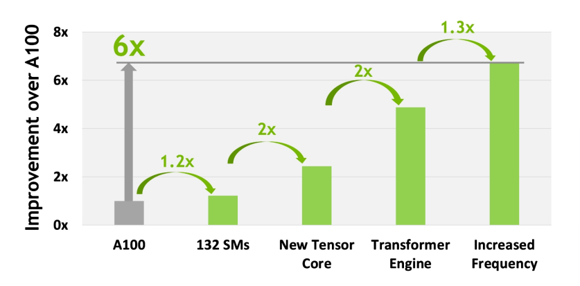
Considering all the new performance improvements in H100, firstly, its SM count is increased by 22% compared to A100, and the speed of each H100 SM is doubled. At the same time, in each Tensor Core, the new FP8 format and related Transformer engine provide an additional 2x improvement. Finally, H100’s higher frequency also provides about 1.3x performance improvement. In summary, H100’s computing performance is about 6x higher than A100.
H100 can be deployed in various data centers, including internal private clouds, public clouds, hybrid clouds, and edge data centers. The product is expected to be fully released later this year. Manufacturers are expected to introduce various servers equipped with H100 accelerators, including Atos, BOXX Technologies, Cisco, Dell, Gigabyte, and Inspur, etc.
This article is a translation by ChatGPT of a Chinese report from 42HOW. If you have any questions about it, please email bd@42how.com.