This article is reproduced from Zhihu author: Yin Wei
As we discussed last time, understanding the significance of automatic driving chips requires not only understanding chip principles, but also understanding that computing is not just a software job, but a collaboration between software and hardware. Many algorithms can be implemented on different chips, but a trade-off between flexibility and cost-power consumption must be made during mass production. And to achieve this, you must understand the chip.
Conceptual Structure of the Chip
Current chip structures are complex, but can be simply divided into three conceptual structures: von Neumann structure, Harvard structure, and modified Harvard structure. Understanding the core structure of a chip means looking at its bus layout and memory design.
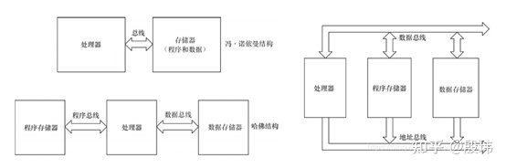
To give an example, if a chip is a “bank,” and this bank is small with only two people. One person is responsible for the abacus (computation), and doesn’t do anything else. The other person is responsible for keeping records (storage), and completely records “What needs to be calculated?” (data) and “How to calculate it?” (program) in the document, which is convenient for communication with the person handling the abacus. They define a communication method between them (a group of buses), which includes two main parts: “Where to get the document? Where to return it?” (address bus) and “What is the specific content of the document?” (data bus). In other words, a group of buses includes an address bus and a data bus. It’s important to note that the “data” on the bus here corresponds to a document, not to be confused with the concept of “What needs to be calculated?” in the document.After the customer hands over the original requirements document (including input data and program) to the responsible recording person, according to the defined communication method, the document is passed back and forth repeatedly with the person responsible for the actual calculation (getting program instructions, getting data, returning results), and finally the final calculation results are fed back to the customer through the recording person. The above division of labor idea is the core of von Neumann architecture, and the key feature is that the customer only needs to communicate with one recording person, even the most complex requirements can be given to one person, and the rest is between them. The entire process is very flexible, which is also the biggest advantage of von Neumann architecture.
In this structure, the program instruction storage address and the data storage address that point to different physical locations in the same memory have the same width. However, this method is not efficient because the recording person can only do one thing at a time, either telling the abacus person how to calculate, or telling it what to calculate. Therefore, the Harvard architecture appeared, separating the storage of program instructions and data, and allowing different widths for instructions and data. Independent sets of program buses and data buses were used. This is equivalent to the original two people, now three people, and the recording person has split the work, one responsible for recording and transmitting the calculation method (program), and one person responsible for recording and transmitting the calculation content (data).
Two people communicate point-to-point with the abacus person, but they cannot communicate with each other. This parallelization naturally improves efficiency. Things that used to take at least two cycles are now completed in one cycle. However, this method requires the customer to correspond to two unrelated recording personnel at the same time, which is very unfriendly. In addition, if the focus of the requirements is different, the workload of the two people is often unbalanced, leading to waste. If one person is responsible (von Neumann architecture), these problems do not exist.
To solve this balance problem, the Modified Harvard Architecture was introduced. It only uses one set of buses for the program memory and data memory to share in time. The original Harvard architecture required four (2 sets) of buses, but the modified architecture only needs two (1 set) of buses while preserving the two independent parallel memories. That is to say, the recording person still divides the work for efficiency, but the communication method has been upgraded and embarked on the “agile road”. It is no longer the model of communication between the two pairs of people like old state-owned enterprises. The customer and the abacus person are also included in a four-party communication meeting (time-sharing sharing), which guarantees flexibility while also having little impact on parallelization.
After discussing the basic structural ideas, there are several points to emphasize. Actual chip design is an expansion and nesting of these conceptual structures. For example, although the external bus of the CPU processor appears to be a von Neumann architecture, due to the design of its internal high-speed cache, it is actually a modified Harvard architecture.
Chip Factional DivisionNext, let’s talk about the classification of chips. Firstly, it is necessary to distinguish the two major categories of chips: general-purpose chips (CPU, GPU, DSP, etc.) and customized chips (FPGA, ASIC, etc.). This classification is very important because the two have fundamentally different characteristics. To use the analogy of a bank, general-purpose chips are like “bank tellers,” while customized chips are like “ATMs.”
The key to general-purpose chips is the word “general.” This means that it must be capable of processing a wide variety of instructions and handling requests from multiple external devices at the same time. It must be able to interrupt the current operation at any time and switch to other operations, then resume the current operation from the interrupt point. This is similar to a bank teller who has to deal with all kinds of business requests from customers, including some who may cut in line or cause trouble. To achieve this, general-purpose chips have a complex control instruction fetch and decode mechanism, a cache memory hierarchy system (to balance the temporary instruction storage between high-speed CPUs and low-speed memory), and a relatively small proportion of actual computing unit (ALU) design. The majority of the design is for flexibility, sacrificing computing efficiency for versatility.
Computing components cannot understand the instructions we give them. They can only understand the two states of a transistor: “on” and “off,” which correspond to 1 and 0 respectively. In order to translate the instructions we give into something the CPU can understand, the CPU needs a specialized decoder to translate our instructions. This process consists of two steps: “instruction fetch” (extracting the instructions that need to be executed from a special memory that stores instructions) and “instruction decode” (translating the instruction into data that the computing unit can understand according to specific rules).
When discussing the structure of chips in the previous section, we focused primarily on the structure of general-purpose chips and the discussion of which “organizational structure and communication methods” are the most efficient when meeting changing customer needs.
Customized chips, on the other hand, are a completely different concept. Although they also involve structural considerations, discussing the “organizational structure” of a program is like discussing the specific timing, interruption, instruction fetch, and decode concepts that are designed for flexibility but don’t exist in this type of chip. Compared to general-purpose chips, customized chips have no “humanity.” They are like ATMs, with clearly defined operations for customers and without a great deal of flexibility designed in, as there’s no need to flirt with the machine.# Comparison of Custom Chips and General-purpose Chips in the Field of Signal Processing
If we take the example of implementing a comparison logic using a von Neumann structure CPU, it would require several instructions to be executed, however, with FPGA, there is no need to consider timing cycles as a few logic units can be connected and the computation can be completed within one cycle. However, if several more logic units are added, the CPU will still complete the computation using a few instructions within the same logic resources, but the FPGA would require additional logic resources to complete the computation.
Similarly, FPGA and GPU have similar ideas in parallelism, but they are actually not comparable. One cannot compare the processing channels of three bank tellers and an ATM with three precisely parallel processes. Also, comparing DSP and FPGA in signal processing efficiency does not make much sense either. The comparisons between these different technologies are not very meaningful as they serve different purposes.
Custom chips operate on fixed business processes and aim to reduce costs and increase efficiency, for instance, banks use ATMs to replace more expensive tellers to perform some routine banking tasks. General-purpose chips, on the other hand, are designed for flexible use cases where specific processes are not yet defined or their definition is subject to change. They serve different aspects of technology and cannot be directly compared based on performance or efficiency.
Having understood the two different directions chips can take, let’s take a closer look at the subcategories, and how CPU (MPU), GPU, DSP, and MCU differentiate within general-purpose chips.
CPU and MPU can be understood as almost the same concept, with differences essentially limited to their scope of application. The main difference between CPU and GPU lies in the number of their cores. Although a CPU may have multiple cores, it is generally limited to less than two digits, with each core having a large enough cache, a sufficient number of digital and logical operation units, and more complex logical judgment hardware. It is good at handling complex customer transactions just like the 3-4 tellers available in banks. In contrast, GPU has far more cores than CPUs, with relatively smaller cached sizes for each core, fewer and simpler digital logic operation units, and more than 500 telephone customer service representatives handling a relatively simple but large number of customer transactions.DSP (digital signal processing chip) is a special type of CPU that uses the Harvard architecture mentioned above and has dedicated hardware algorithm circuits and specialized addressing modes. It has the flexibility of a general chip design but rarely changes during real-time operations, so it specializes in the performance of business processes (recording and calculation). It is like the deployment of specialized clerks and processes for a “foreign exchange access” professional counter. DSP’s ability to process dedicated signals (video coding, communication signals) far exceeds that of general-purpose CPUs. Of course, ordinary counters can also handle the business of promotion counters, but the cost-effectiveness is poor. If there are many requirements, it makes sense to set up a dedicated counter, which still depends on customer demand. Processing specialized signal flows with DSP often has advantages such as controllable execution time and high chip cost-effectiveness.
After discussing general chips, there are also two main directions for customized chips, FPGA and ASIC. The core difference between the two is the degree of solidification. FPGA still has a certain degree of flexibility (but far inferior to general chips), while ASIC completes the solidified design (there are also products similar to FPGA with partial editing). It is similar to programmable ATMs and fully solidified ATMs, and the biggest difference between the two is still cost and power consumption.
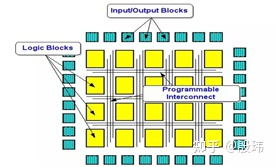
FPGA was originally developed from specialized integrated circuits and is a semi-customizable programmable circuit, which is a high-end CPLD (complex programmable logic device). FPGA can achieve the functions of a DSP, GPU, or even a CPU, just like the clerk business is solidified into ATM operation processes as mentioned earlier. But this does not mean that FPGA can replace the CPU, which is a major difference in design purpose, which is repeatedly emphasized.
FPGA is a bunch of logic gates that are connected into a circuit from the most basic logic gate level through hardware description language HDL. Although it looks like a CPU, it is actually completely hardware implemented. It processes input data according to a fixed pattern and then outputs it. Most of the FPGA chips are computing units, and there is no control unit, which does not mean that FPGA will not execute instructions. In fact, the control unit in FPGA is completed by the programmable logic connection lines between units, and the operation logic and connection methods of each unit are changed through HDL programming, so that it can achieve similar effects to running programs normally. Since the steps of instruction fetching and decoding by the CPU are omitted, the efficiency of repeatedly running the same code on FPGA is greatly improved. Therefore, it cannot respond to instructions that have not been programmed.ASIC stands for Application-Specific Integrated Circuit, which has no clear definition. It can be understood as any IC that is not as well-known as a microcontroller, DSP, or FPGA, and everything else is ASIC. ASIC was originally developed as a specialized integrated chip for a specific function. Later, ASIC developed into a semi-custom integrated circuit, which is relatively similar to FPGA. In some places, ASIC is a broad concept, and FPGA is part of ASIC, and is often used as a pre-research for ASIC development. It represents the ultimate pursuit of cost-effectiveness under certain requirements.
Integration of chips
I secretly left out a concept, MCU, above, because it is not a type of chip but a way of integration, and the same goes for SOC chips. The difference between the two lies in the degree of integration. In the autonomous driving field, MCU integrates more input and output devices into the chip, making it easier to control, so it is called a microcontroller rather than a microprocessor. SOC integrates different chips at a higher level, with higher dimensions. If MCU is a personnel organization forming a company to serve externally, then SOC is more like an industry formed by company-level organizations serving externally.
Microcontroller is a popular term for MCU. The classic 51 series is just a bunch of IO ports, and later gradually added commonly used functionalities such as PWM, AD, etc. Its structure is equivalent to a CPU with more external peripherals, but the focus is on discussing its external peripherals. Continuing to develop external peripherals such as PWM and AD forms the ECU familiar to the automotive industry, which is the Electronic Control Unit, and also refers to all electronic control systems in the vehicle, such as steering ECU, air conditioning ECU, etc.
ECU generally consists of MCU, expanded memory, expanded input and output (CAN/LIN, AD, PWM, etc.), power circuit, and some other electronic components. Specific functional ECU also has components such as infrared transceiver, pulse generator, strong and weak electrical isolation, etc. The entire circuit board is designed and installed in an aluminum box and can be conveniently installed on the vehicle body sheet metal by snaps or screws.
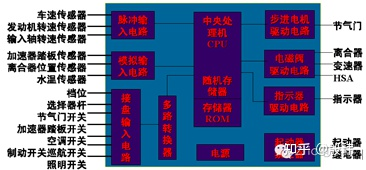
In the input processing circuit, ECU’s input signals are mainly in three forms: analog signals, digital signals (including switch signals), and pulse signals. The analog signal is converted into a digital signal by A/D conversion and provided to the microprocessor.In the output circuit, the signals output by the microprocessor are often used to control actuators such as solenoid valves, indicator lights, and stepping motors. The power of the microprocessor output signal is small, using +5V voltage, while the power supply of the actuators on the car is mostly from the battery. Therefore, the control signal of the microprocessor needs to be processed through the output processing circuit (D/A, amplification, etc.) before driving the actuators.
In the power circuit, the ECU of traditional cars usually has a battery and built-in power circuit to ensure that the microprocessor and its interface circuit work at +5V voltage. Even when the battery voltage fluctuates greatly, it can provide stable voltage to ensure the normal operation of the system.
Generally, ECU equipped with 8-bit MCU is mainly used for low-level control functions such as fan control, air conditioning control, wiper, sunroof, and door control. 16-bit MCUs are mainly used for engine control, gear and clutch control, etc. 32-bit MCUs are used for multimedia information systems, real-time safety and power systems, and complex X-by-wire transmission functions. More complex functions are not within the scope of MCU or ECU discussions.
With the development of autonomous driving, the concept of ECU has been further upgraded, and the more popular term is domain controller, which is nothing more than turning MCU into SoC (System on Chip) and integrating more peripheral devices. Currently, the mainstream general-purpose chips (GPP) carried by domain controllers mostly adopt the SoC chip design method, and various functional chips are integrated into circuits through HDL language. In SoC, various components (IP cores) are combined together like building blocks. IP cores (such as typical ARM core design technology) are licensed to hundreds of semiconductor manufacturers to make different SoC chips. They may also integrate GPU, codec (DSP), GPS, WiFi, Bluetooth baseband, and a series of functions. If you take a look at chips from Qualcomm or TI, they basically have an ARM core controlling overall operations, a DSP processing voice encoding and decoding, a GPU responsible for image processing, a baseband and antenna processing module responsible for communication, as well as GPS, security encryption, and other special chips.
In the past, the prototype processors of fully autonomous driving could consume up to 5000W of power, which was not only expensive but also required additional heat dissipation devices. The development of SoC and ASIC has brought us many inspirations, returning to the flexibility that runs through the entire autonomous driving system that I often mention. In the new SoC world, you will not assemble physical components from different suppliers. Instead, you assemble IP from different suppliers to obtain better integration, thus making it easier to reduce power consumption and costs.
Software-Hardware Matching DesignMost autonomous driving algorithm companies want to customize or make their own ASIC/SOC computing platforms, for another reason related to the match between software and hardware. The performance of algorithms is often dependent on hardware design. Pursuing modularity means sacrificing utilization. Improving utilization requires integrated software and hardware design. The design of chips should consider whether the algorithm is suitable for GPU or CPU, how much memory and MAC are needed for network models at once. Conversely, given a chip, how should the algorithm be compatible and whether to reduce memory access times to improve utilization or to migrate some CPU-based rule-based algorithms to GPU-based deep learning implementations. Software and hardware must be considered together in order to fully utilize system performance.
Different chips, algorithms, and requirements often have an optimal combination. For example, when a classic and commonly used algorithm application requires a large amount and intense competition, ASIC is a good choice. It is foolish to pay for an ARM license for a simple function such as encoding and decoding.
If an algorithm is very classic and low-level, but there is still room for improvement and adaptation to different scenarios, signal stream processing (such as mobile voice processing) can be directly performed using DSP, while more complex input-output logical algorithms (such as image SIFT feature processing) can be done by FPGA, which increases performance by 30-100 times compared to CPU, with lower costs and energy consumption.
In the field of complex algorithms, compared to CPU, the parallel architecture of GPU sends the same instruction flow to multiple cores for parallel execution with different input data. Therefore, GPU is more suitable for parallel algorithms while CPU is more suitable for serial complex logical processing. Specifically, if a scalar is regarded as a zero-order tensor, a vector as a first-order tensor, and a matrix as a second-order tensor. CPU corresponds to scalar calculations, mainly for path planning and decision-making algorithms, and commonly used sensor fusion such as Kalman filter algorithms are mostly scalar operations. GPUs correspond to vector, or vector, computations, including point clouds, maps, and deep learning, and are primarily focused on matrix operations. When writing programs in CPU, it is more suitable to improve performance by leaner logic, while when writing programs in GPU, it is more suitable to use algorithm concurrent processing to improve performance.
With this level of understanding, most work related to chips can be carried out.
This article is a translation by ChatGPT of a Chinese report from 42HOW. If you have any questions about it, please email bd@42how.com.